Memory cell device and manufacturing method

a memory cell and manufacturing method technology, applied in semiconductor devices, digital storage, instruments, etc., can solve the problems of manufacturing such devices with very small dimensions, and achieve the effect of facilitating the change of an electrical property sta

Active Publication Date: 2009-10-06
MACRONIX INT CO LTD
View PDF333 Cites 7 Cited by
  • Summary
  • Abstract
  • Description
  • Claims
  • Application Information

AI Technical Summary

Benefits of technology

[0010]A first aspect of the invention is directed to a memory cell device of the type including a memory material switchable between electrical property states by the application of energy. The memory cell device comprises a first electrode having an electrode surface. A first material is over the electrode surface to create a separation layer having an upper surface. The first material defines a hole bounded by a side wall within the separation layer, a bottom, and a plane defined by the upper surface. A second material and is on the side wall with the second material defining a void. The void has a downwardly and inwardly tapering void region below the plane of the upper surface. A memory material is in at least a portion of the void region and is in electrical contact with the electrode surface. A second electrode is an electrical contact with the memory material. Energy passing between the first and second electrodes is concentrated within the memory material so to facilitate changing an electrical property state of the memory material. In some embodiment the memory material comprises a phase change material. The second material may comprise a high density plasma-deposited material.
[0011]A second aspect of the invention is directed a method for making a memory cell device of the type including a memory material switchable between electrical property states by the application of energy. They first electrode is formed, the first electrode having an electrode surface. A first material is deposited over the electrode surface to create a separation layer having an upper surface. A hole is formed through the separation layer. The hole is bounded by a side wall within the separation layer, a bottom, and a plane defined by the upper surface. A deposition procedure is selected. A second material is deposited on the side wall using the selected procedure. The selecting and second material depositing steps are carried out so that the second material defines a void. The void has a downwardly and inwardly tapering void region below the plane of the upper surface. A memory material is deposited in at least a portion of the void region and in electrical contact with the electrode surface. A second electrode is formed in electrical contact with the memory material. Energy passing between the first and second electrodes is concentrated within the memory material so to facilitate changing an electrical property state of the memory material. In some embodiments the selecting step comprises selecting a high density plasma chemical vapor deposition (HDP CVD) procedure and the depositing step comprises depositing, using the selected HDP CVD procedure, the second material on the side wall.

Problems solved by technology

Problems have arisen in manufacturing such devices with very small dimensions, and with variations in process that meet tight specifications needed for large-scale memory devices.

Method used


Image

  • Memory cell device and manufacturing method
  • Memory cell device and manufacturing method
  • Memory cell device and manufacturing method

Examples


Embodiment Construction

[0020]The following description of the invention will typically be with reference to specific structural embodiments and methods. It is to be understood that there is no intention to limit the invention to the specifically disclosed embodiments and methods but that the invention may be practiced using other features, elements, methods and embodiments. Like elements in various embodiments are commonly referred to with like reference numerals.

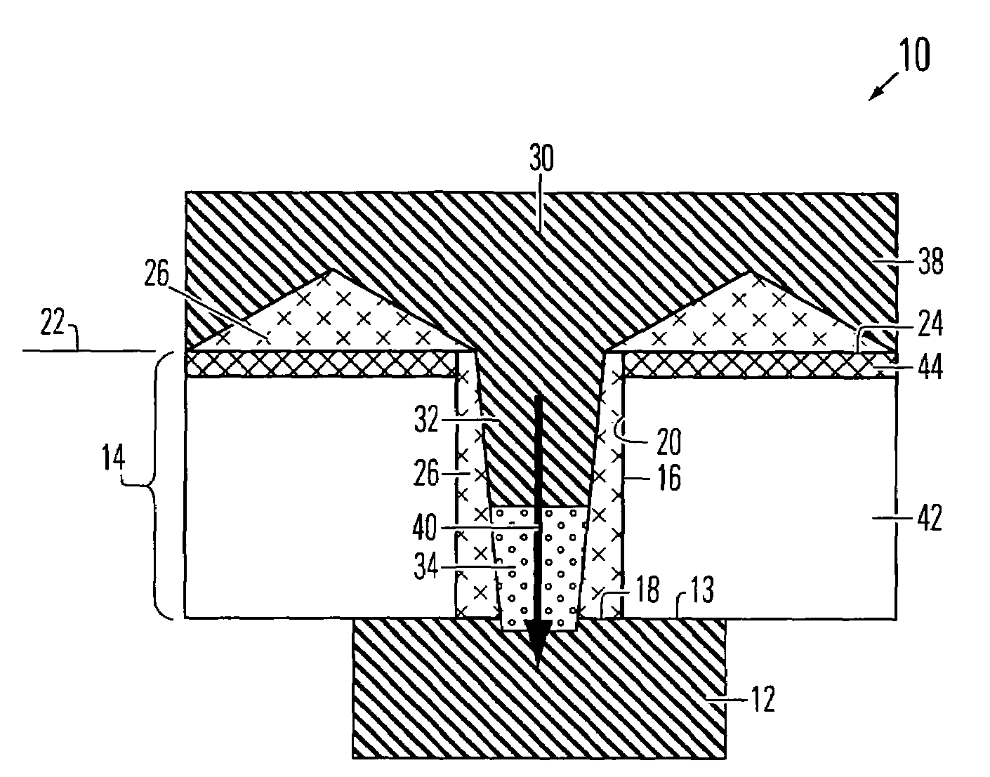
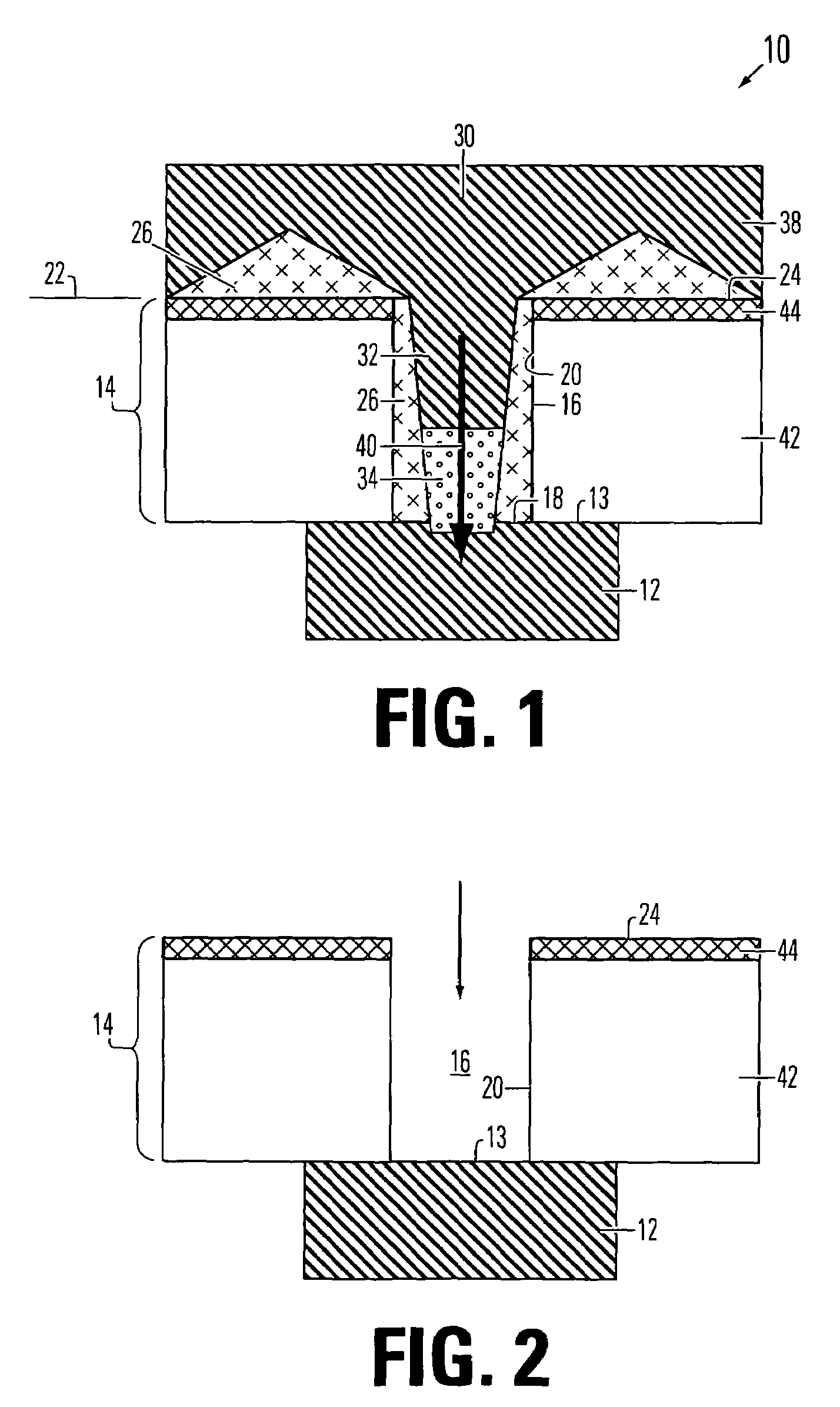
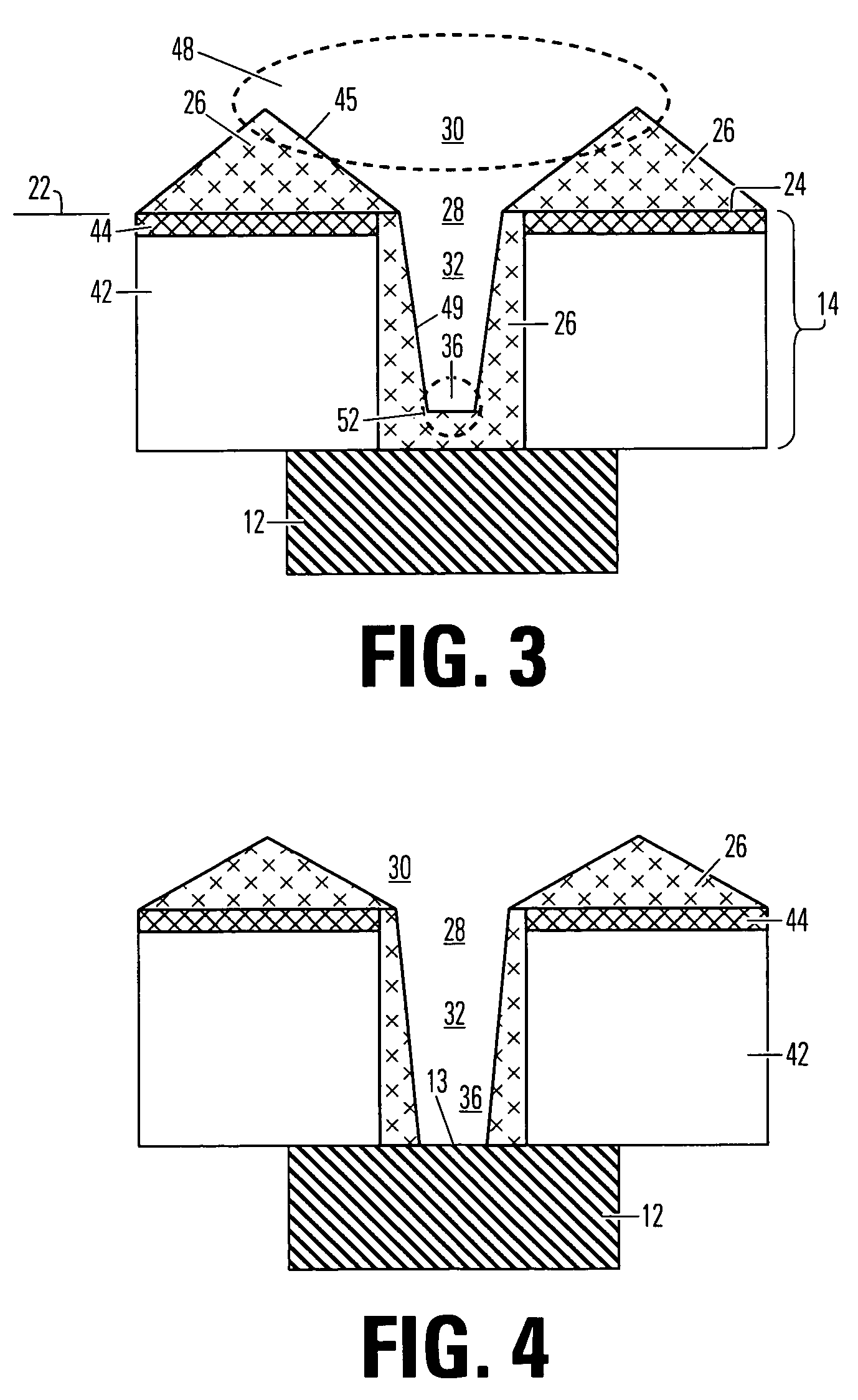
[0021]FIG. 1 is a simplified cross-sectional view of a memory cell device 10 made according to one embodiment of the invention. Device 10 comprises broadly a first, bottom electrode 12 having an electrode surface 13 onto which a separation layer 14 is deposited. A hole 16 is formed through separation layer 14 down to first electrode 12. Hole 16 is bounded by a bottom 18, a side wall 20 and a plane 22 defined by the upper surface 24 of separation layer 14. A material 26 is deposited on upper surface 24, side wall 20 and bottom 18 preferably using ...


PUM


Abstract

A memory cell device, having a memory material switchable between electrical property states by the application of energy, comprises an electrode, a separation layer against an electrode surface, a hole in the separation layer, a second material in the hole defining a void having a downwardly and inwardly tapering void region. A memory material is in the void region in electrical contact with the electrode surface. A second electrode is in electrical contact with the memory material. Energy passing between the first and second electrodes is concentrated within the memory material so to facilitate changing an electrical property state of the memory material. The memory material may comprise a phase change material. The second material may comprise a high density plasma-deposited material. A method for making a memory cell device is also discussed.

Description

CROSS REFERENCE TO RELATED APPLICATIONS[0001]This application claims the benefit of provisional patent application No. 60 / 738,924 filed 22 Nov. 2005.BACKGROUND OF THE INVENTION[0002]1. Field of the Invention[0003]The present invention relates to high density memory devices based on memory materials, for example resistor random access memory (RRAM) devices, the memory material switchable between electrical property states by the application of energy. The memory materials may be phase change based memory materials, including chalcogenide based materials and other materials, and to methods for manufacturing such devices.[0004]2. Description of Related Art[0005]Phase change based memory materials are widely used in read-write optical disks. These materials have at least two solid phases, including for example a generally amorphous solid phase and a generally crystalline solid phase. Laser pulses are used in read-write optical disks to switch between phases and to read the optical prope...

Claims


Application Information

Patent Timeline
Patent Type & Authority Patents(United States)
IPC IPC(8): G11C11/00
CPCH01L45/04H01L45/1233H01L45/126H01L45/144H01L45/06H01L45/1246H01L45/1691H01L45/146H01L45/147H01L45/148H01L45/1625H01L45/1641H01L45/14H10N70/828H10N70/20H10N70/881H10N70/8836H10N70/231H10N70/884H10N70/026H10N70/041H10N70/068H10N70/8828H10N70/8833H10N70/826H10N70/8413
Inventor LAI, ERH-KUNHO, CHIAHUAHSIEH, KUANG YEU
Owner MACRONIX INT CO LTD
Why Eureka
Try Eureka