Semiconductor substrate transfer apparatus and semiconductor substrate processing apparatus equipped with the same

a technology of semiconductor substrate and transfer apparatus, which is applied in the direction of instruments, packaged goods, program control, etc., can solve the problems of limiting the number of wafers stored in the storage container, and not realizing a satisfactory transfer throughput depending on conditions

Active Publication Date: 2009-11-17
ASM JAPAN
View PDF20 Cites 390 Cited by
  • Summary
  • Abstract
  • Description
  • Claims
  • Application Information

AI Technical Summary

Problems solved by technology

Although the transfer robot combining the above-mentioned method of transferring plural wafers all at once and the dual-arm method is effective, it may not realize a satisfactory transfer throughput depending on conditions.
Because of this, there was a limit to the number of wafers stored in the storing container.

Method used


Image

  • Semiconductor substrate transfer apparatus and semiconductor substrate processing apparatus equipped with the same
  • Semiconductor substrate transfer apparatus and semiconductor substrate processing apparatus equipped with the same
  • Semiconductor substrate transfer apparatus and semiconductor substrate processing apparatus equipped with the same

Examples


Embodiment Construction

[0045]The present invention will be explained with reference to preferred embodiments and drawings. However, the preferred embodiments and drawings are not intended to limit the present invention.

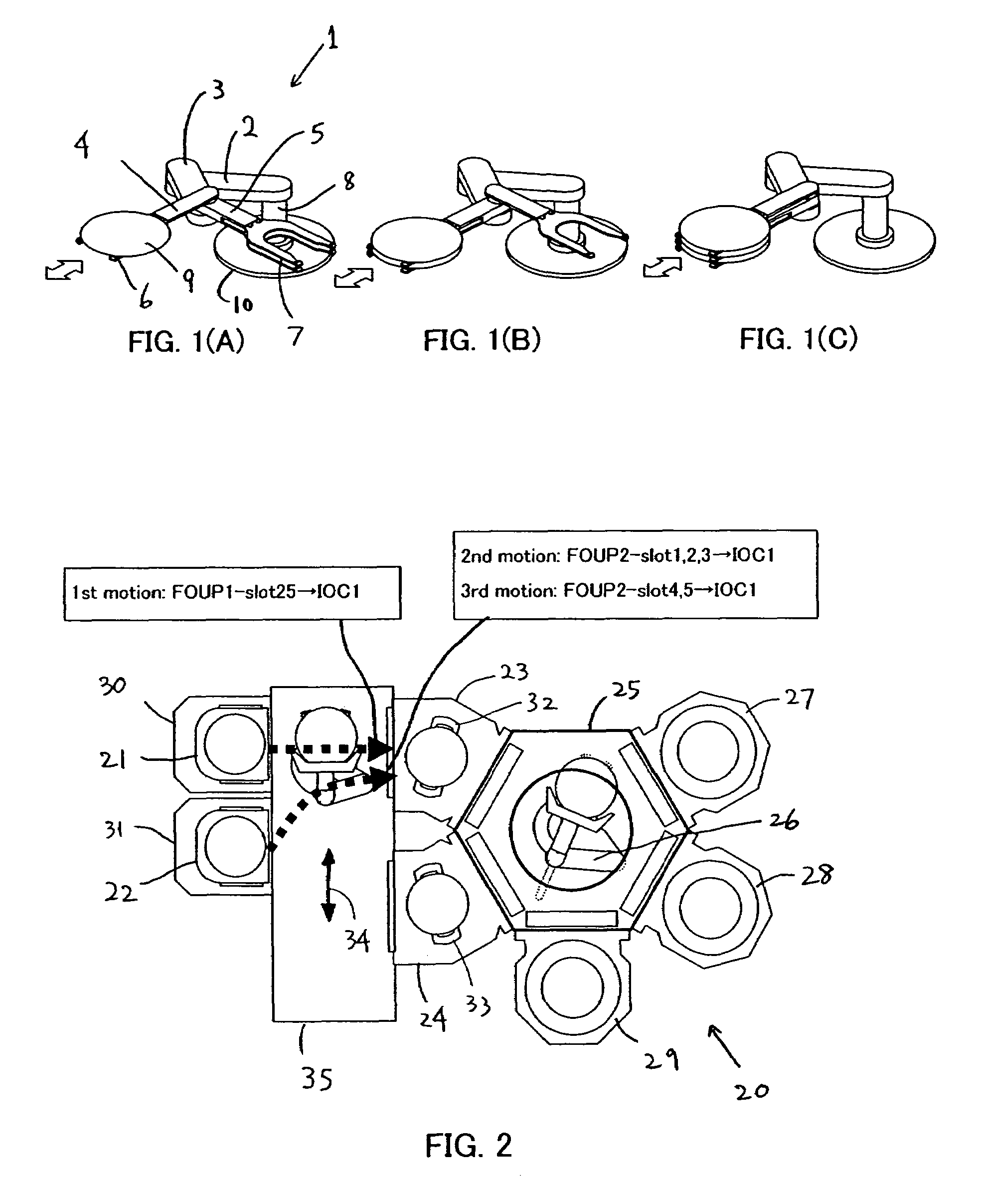
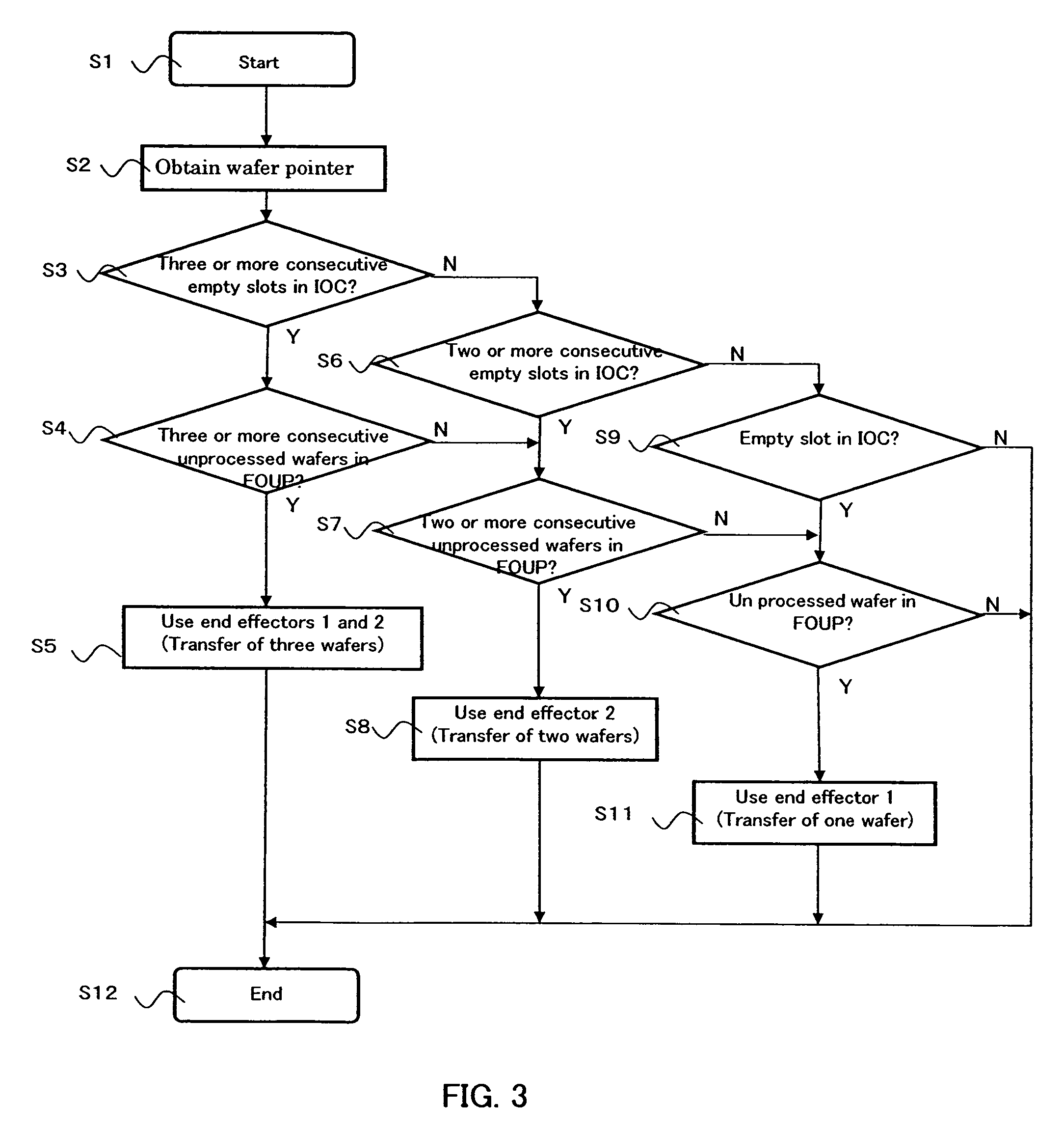
[0046]In an embodiment of the present invention, a semiconductor substrate transfer apparatus comprises at least one arm and N (N is any integer of two or more) end effectors rotatably joined with the arm, each of which end effector holds at least one semiconductor substrate, which is characterized in that at the start of a substrate transfer process, at least one desired end effector is selected from N end effectors according to a substrate distribution status in a transfer origin and an empty slot status in a transfer destination, a selected end effector and an unselected end effector rotate independently of each other in respect to the arm, and a semiconductor substrate is transferred by the selected end effector.

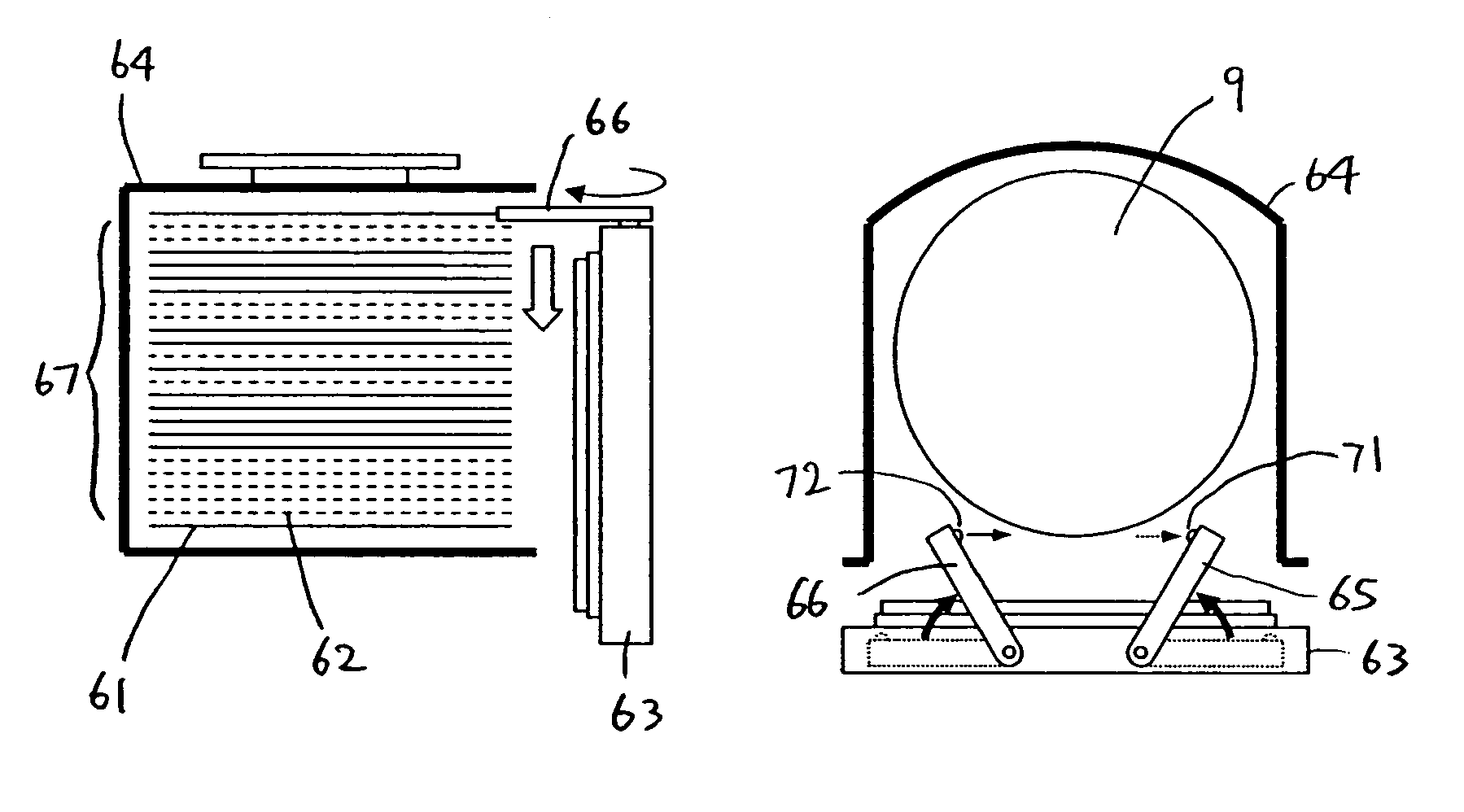
[0047]Preferably, N equals 2 and a first end effector holds one semiconduct...


PUM


Abstract

A semiconductor substrate transfer apparatus for transferring semiconductor substrates from a first container to a second container, includes: multiple end effectors; at least one robot arm with which the multiple end effectors are independently rotatably joined; and a controller storing software including instructions to judge which end effector or end effectors in the multiple end effectors are to be selected based on a distribution status of substrates stored in the first and second containers and to rotate the selected end effector(s) for unloading a substrate or substrates from the first container and loading the substrate or substrates to the second container.

Description

BACKGROUND OF THE INVENTION[0001]1. Field of the Invention[0002]The present invention generally relates to a semiconductor substrate processing apparatus; particularly to a semiconductor substrate transfer apparatus for carrying in / out a semiconductor wafer between a storing container and a processing container.[0003]2. Description of the Related Art[0004]In a semiconductor processing apparatus, a semiconductor wafer normally has to be transferred between plural separate containers inside the apparatus in order to deliver the wafer from a storing container to a processing container in which a target process is performed. As this type of mechanism for transferring a semiconductor wafer, a transfer robot is widely known. In conventional semiconductor processing apparatuses, there are many different types of transfer robots having various shapes and motion forms in order to meet the apparatuses' purposes and requirements.[0005]In recent years, in semiconductor production, a throughput ...

Claims


Application Information

Patent Timeline
Patent Type & Authority Patents(United States)
IPC IPC(8): B65B69/00
CPCH01L21/67265H01L21/67276H01L21/67781H01L21/68
Inventor TAKIZAWA, MASAHIROSUWADA, MASAEIWADA, TAKASHI
Owner ASM JAPAN
Why Eureka
Try Eureka