Compact camera module and the substrate thereof

a camera module and compact technology, applied in the field of compact camera modules and their substrates, can solve the problems of image distortion of compact camera modules, inability to precisely align with the center of lens modules, etc., and achieve the effect of facilitating self-checking the relative position

Inactive Publication Date: 2009-11-24
ADVANCED SEMICON ENG INC
View PDF3 Cites 0 Cited by
  • Summary
  • Abstract
  • Description
  • Claims
  • Application Information

AI Technical Summary

Benefits of technology

[0008]It is an object of the present invention to provide a compact camera module and the substrate thereof. The substrate includes a plurality of check bars disposed outside the chip-attached area. The intersection point of the perpendicular bisectors of the check bars aligns with a check point defined on the substrate so as to facilitate self-checking the relative position of the sensor area of the sensor chip to the substrate and / or a lens module, thereby ensuring the center of the sensor area aligns with the intersection point of the perpendicular bisectors. In addition, the check bars can be functioned as reference points to help to precisely attach the sensor chip to the predetermined position in the chip-attached area.
[0009]In accordance with the present invention, a compact camera module includes a substrate, a sensor chip and a lens module. The substrate has an upper surface defining a chip-attached area adapted to receive the sensor chip attached thereon and a module-secured area adapted to carry the lens module mounted thereon. The module-secured area surrounds the chip-attached area and a check point is defined in the chip-attached area. The substrate includes a plurality of connecting pads and a plurality of check bars disposed outside the chip-attached area. The perpendicular bisectors of the check bars intersect with each other at a point that aligns with the check point. Therefore, the check bars can help to self-check whether the center of the sensor area of the sensor chip aligns with the check point.

Problems solved by technology

However, the use of the fiducial marks 115 to assist to attach the sensor chip to the chip-attached area 112 is apt to cause the center of the sensor area of the sensor chip not to be placed in the predetermined position and therefore cannot precisely align with the center of the lens module.
This will cause the image distortion of the compact camera module.

Method used


Image

  • Compact camera module and the substrate thereof
  • Compact camera module and the substrate thereof
  • Compact camera module and the substrate thereof

Examples


Embodiment Construction

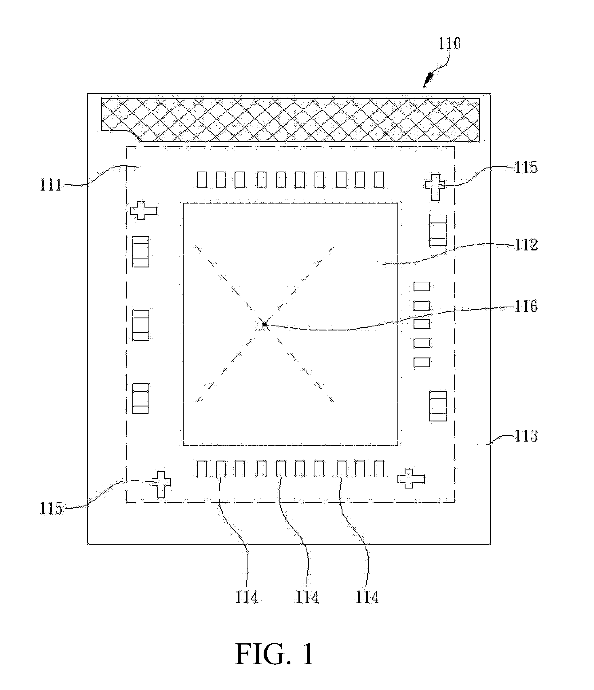
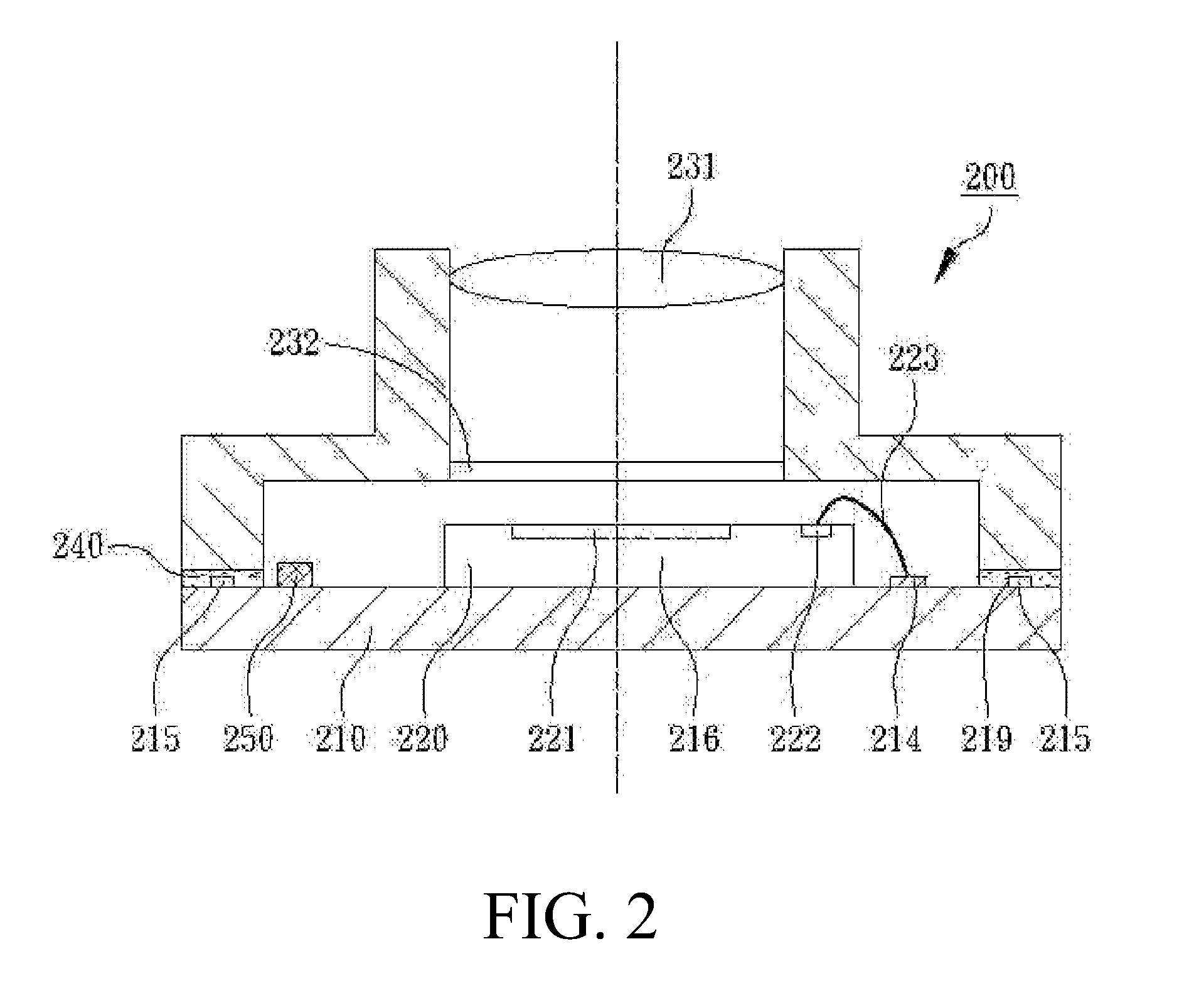
[0015]FIG. 2 illustrates a cross-sectional view of a compact camera module according to one embodiment of the present invention. FIG. 3 illustrates a top view of a substrate for compact camera modules and FIG. 4 illustrates a top view of the substrate of FIG. 3 with a chip attached thereon.

[0016]Referring to FIG. 2, the compact camera module 200 includes a substrate 210, a sensor chip 220 and a lens module 230. The substrate 210 is a chip carrier and the sensor chip 220 and lens module 230 are disposed on the upper surface 211 of the substrate 210. In this embodiment, the sensor chip 220 is a CMOS sensor chip that has a sensor area 221 for sensing rays of light and a plurality of contact pads 222. The lens module 230 has a lens 231 and a filter 232. In addition, a plurality of passive components 250 is disposed on the upper surface 211 of the substrate 210.

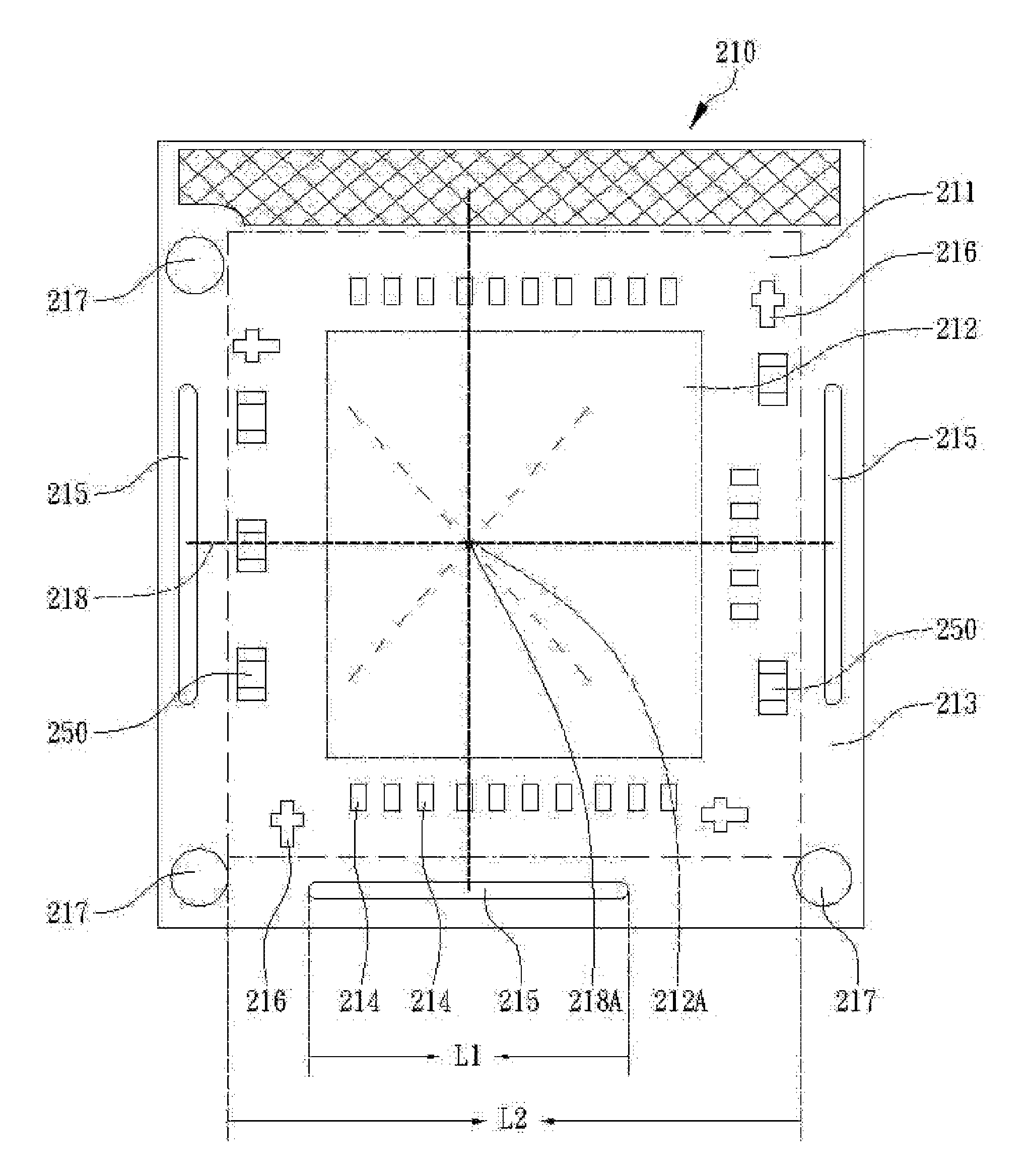
[0017]Referring to FIG. 3, the upper surface 211 of the substrate 210 defines a chip-attached area 212, a module-secured area 21...


PUM


Abstract

A compact camera module (CCM) substantially includes a substrate, a sensor chip and a lens module. The substrate has a surface defining a chip-attached area for attaching the sensor chip and a module-secured area for mounting the lens module. A check point is defined in the chip attached area. The module-secured area surrounds the chip-attached area. The substrate includes a plurality of connecting pads and a plurality of check bars disposed outside the chip-attached area, wherein the perpendicular bisectors of the check bars intersect with each other at a point aligning with the check point. Accordingly, a self-check step can be performed to check the center of the sensor area of the sensor chip in accordance with the intersection point after a chip is attached.

Description

CROSS REFERENCE TO RELATED APPLICATION[0001]This application claims the priority benefit of Taiwan Patent Application Serial Number 095105991 filed Feb. 22, 2006, the full disclosure of which is incorporated herein by reference.BACKGROUND OF THE INVENTION[0002]1. Field of the Invention[0003]The present invention relates to a compact camera module and the substrate thereof, and more particularly, to a compact camera module that can perform a self-check after a chip is attached and the substrate thereof.[0004]2. Description of the Related Art[0005]Compact camera modules (CCMs) are a type of compact image capturer and can be adopted in compact camcorders, digital still cameras or in electronic devices, such as cell phones, laptop computers and hand-held computers. The compact camera module substantially includes an image sensor chip disposed on a substrate and a barrel-shaped lens module with a lens. Rays of light can pass through the lens and reach the sensor area of the image sensor ...

Claims


Application Information

Patent Timeline
Patent Type & Authority Patents(United States)
IPC IPC(8): G03B17/00
CPCG03B17/02H01L27/14618H04N17/002H04N5/2254H04N5/2257H01L27/14625H01L2224/48091Y10S438/975H04N23/57H04N23/55H01L2924/00014
Inventor CHENG, SHE-HONGCHEN, KUO-HUA
Owner ADVANCED SEMICON ENG INC
Why Eureka
Try Eureka