
Cyclic loading system and methods for forming nanostructures

a nanostructure and loading system technology, applied in the field of nanofabrication and/or microfabrication systems and methods, can solve the problems of limited work performed limited options, and limited work on purely mechanical imprinting techniques

Inactive Publication Date: 2009-12-15
TRINITY COLLEGE DUBLIN
View PDF7 Cites 5 Cited by
  • Summary
  • Abstract
  • Description
  • Claims
  • Application Information

AI Technical Summary

Problems solved by technology

For nanometer scaling forming, options have been comparatively limited.
Limited work has been performed on purely mechanical imprinting in which shear stresses generated under normal load are sufficient to induce plastic flow.
Direct mechanical techniques can be used on a larger variety of substances, but these techniques are subject to a number of fidelity limiting issues including ultrahigh extrusion aspect ratios, strain hardening, and elastic relaxations of the bounding surfaces due to the large pressures involved.
However, there are still issues with stability and fidelity of form patters, de-molding and variation of temperature, and multi-layer or multi-step processing.

Method used


Image

  • Cyclic loading system and methods for forming nanostructures
  • Cyclic loading system and methods for forming nanostructures
  • Cyclic loading system and methods for forming nanostructures

Examples


example

Example 1

Shear Based Residual Layer Thinning

[0109]FIGS. 4A and 4B demonstrate shear based residual layer thinning, with an extrusion aspect ration up to 30:1 or more, all at very small lateral shear strains of at most 2%. In this example, a 3 micrometer diameter punch made of silicon thinned an initially 950 nm thick layer of polystyrene from a residual depth (ie. remaining thickness of the film) of 380 nm down to 90 nm according to the amount of oscillating shear force applied. FIG. 4A shows the relative depth of the residual layer (nm) verses the mean relative motion (nmpp). FIG. 4B are atomic force micrographs showing the surface of residual layers and surrounding extruded material that remain after stamp removal for no shear based forming (top) and the maximum (to 90 nm residual thickness) shear based forming. The fine, cross-hatched lines are 60 nm wide replicas of fine, 60 nm wide lines formed on the face of the flat punch used. It can be seen that these fine lines are preserv...

example 2

Residual Film Thickness as a Function of Applied Mean Normal Pressures

[0110]FIG. 5 is a graph of residual film thickness (nm) plotted against piezo drive amplitude (nm), at four different applied mean normal pressures: 75 MPa, 150 MPa, 300 MPa, and 600 MPa. A silicon flat punch of diameter 3 micrometer is used to thin a 950 nm thick film of polystyrene. The graph demonstrates film thinning as a function of applied piezo drive amplitude for each mean normal pressure. As piezo drive amplitude increases, the residual film thickness decreases. The actual stamp-polymer relative motion is about 20% of the drive amplitude, and at most about 1% the width of the stamp.

example 3

Cyclic Shear Loading Improves Extrusion

[0111]A flat punch indented into a 1600 nm polystyrene film to a mean pressure of 550 MPa without oscillation leaves a profile, as shown in FIG. 7. Under the same conditions, but with additional application of lateral sinusoidal loading by applying 10 volts peak-to-peak to a piezoelectric element at a frequency of 1640 Hz (with oscillation), the sheared contact is seen to have an additional 400 nm of extrusion (FIG. 7). The 400 nm increase in extrusion converts to mask ratio improvement from 1600:600=8:3 to 1600:200=8:1, for a significant three fold improvement. The extrusion occurs in a brief instant for example less than 0.1 second upon the application of the oscillating force.


PUM

PropertyMeasurementUnit
sizeaaaaaaaaaa
depthaaaaaaaaaa
depthaaaaaaaaaa

Abstract

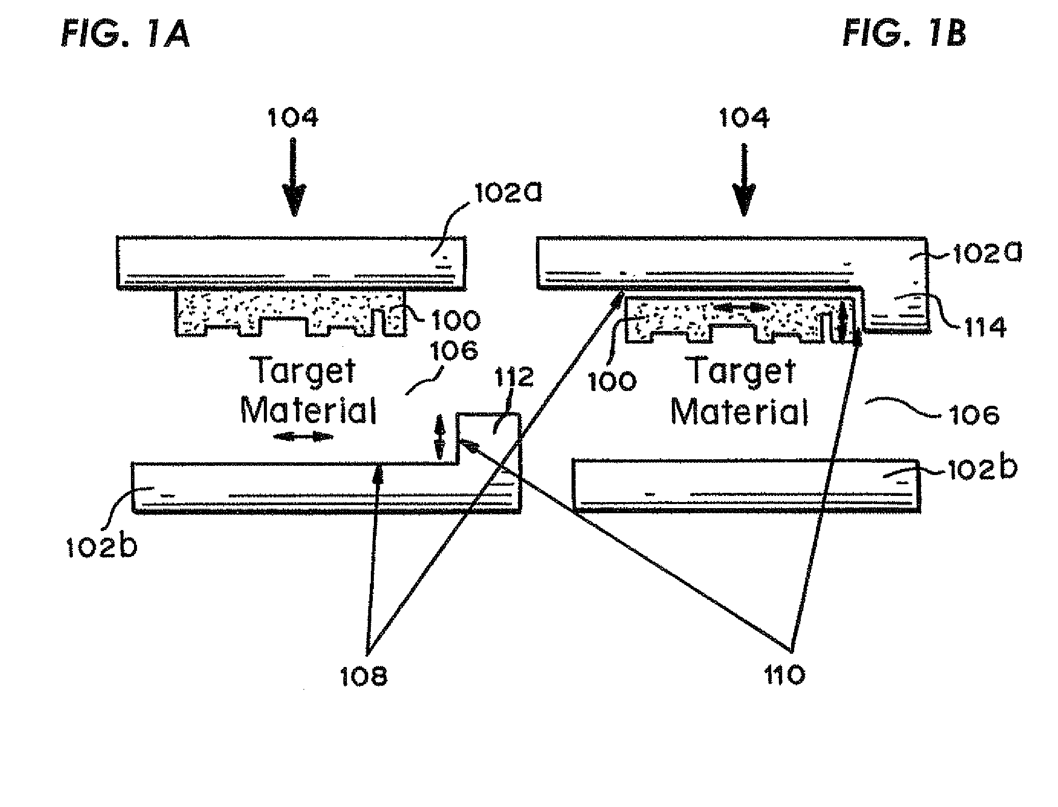
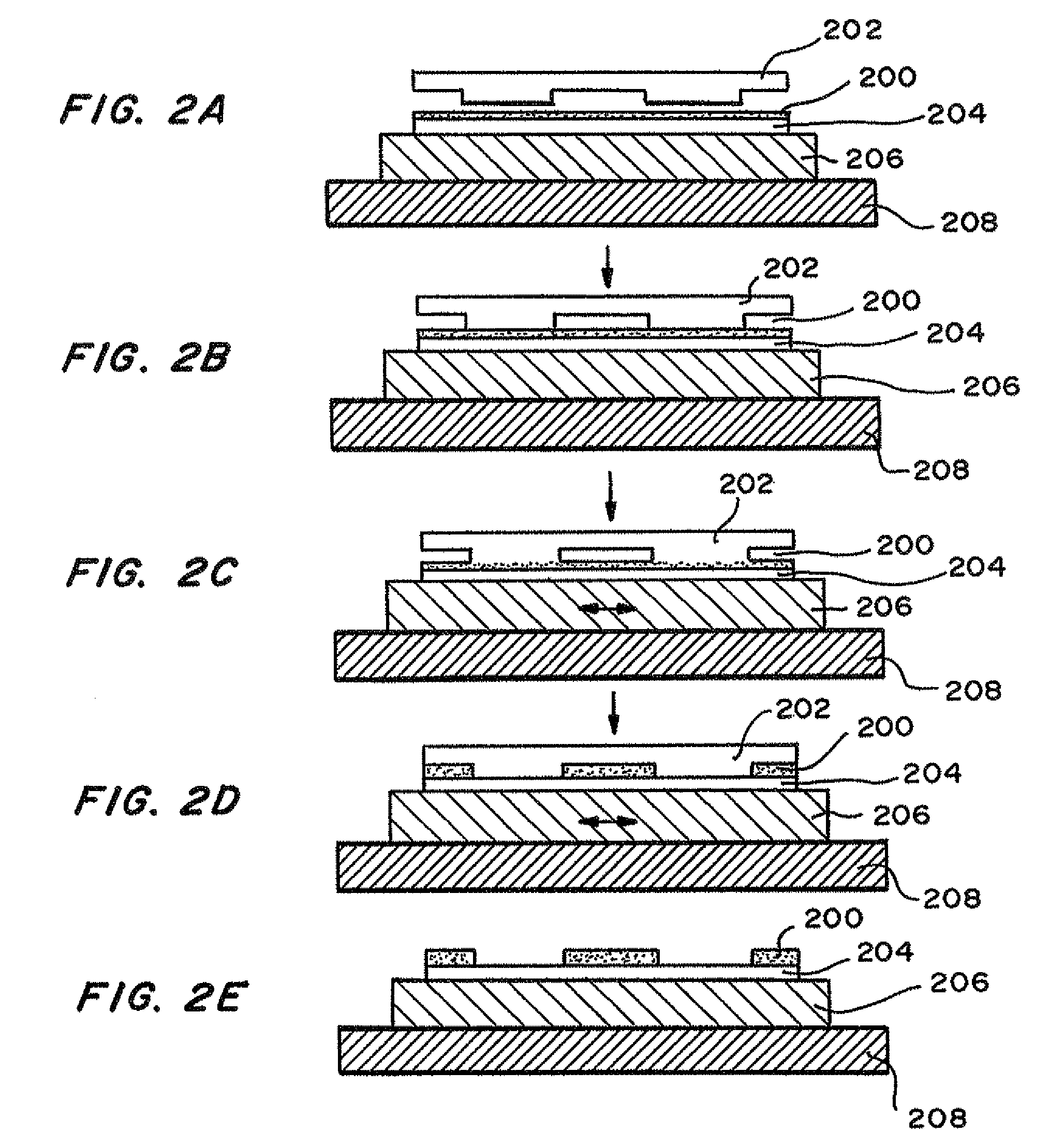
Systems and methods for forming patterns and structures in target materials are described. The method produces a pattern or structure in a target material by contacting a stamp including one or more features with a target material using a normal load sufficient for keeping the one or more features in contact with the target material, and providing a cyclic shear force in an amount sufficient to extrude the target material and form a negative relief of the one more features in the target material. The systems and methods can be used to produce a variety of articles including, but not limited to, semiconductor integrated electrical circuits, integrated optical, magnetic, mechanical circuits and microdevices.

Description

CROSS REFERENCE TO RELATED APPLICATION[0001]This application claims benefit of and priority to U.S. Provisional Patent Application No. 60 / 862,325 filed Oct. 20, 2006, and where permissible is incorporated by reference herein in its entirety.FIELD OF THE INVENTION[0002]Aspects of the disclosure are generally directed to nanofabrication and / or microfabrication systems and methods, and more particularly to systems and methods for forming micro- or nanostructures by direct mechanical contact methods.BACKGROUND OF THE INVENTION[0003]Forming operations are traditionally divided into machining (mass removal, milling, lathing, drilling, and chip production, waste) and deformation (mass conserving, forging, pressing, and rolling at low temperature, and molding at high temperature). For nanometer scaling forming, options have been comparatively limited. Generally, these must be mass preserving and involve unusual geometries. The increased role of surfaces and constitutive behavior may also be...

Claims


Application Information

Patent Timeline
Patent Type & Authority Patents(United States)
IPC IPC(8): B29C59/00
CPCB29C43/003B29C43/021B29C59/022B82Y10/00B82Y40/00G03F7/0002B29C59/026B29C2043/025B29C2043/142Y10T428/24479B29C2043/5833B29C2059/023B29C2043/5825
Inventor PETHICA, JOHN B.CROSS, GRAHAM LAWRENCE WILLIAMOZER, HAKAN OZGURO'CONNELL, BARRY S.
Owner TRINITY COLLEGE DUBLIN
Learn More