Semiconductor chip shape alteration

a technology of semiconductors and chips, applied in the direction of semiconductor devices, semiconductor/solid-state device details, electrical apparatus, etc., to achieve the effects of reducing physical stress, reducing delamination, and dicing efficiency

Inactive Publication Date: 2010-01-19
GLOBALFOUNDRIES INC
View PDF12 Cites 7 Cited by
  • Summary
  • Abstract
  • Description
  • Claims
  • Application Information

AI Technical Summary

Benefits of technology

[0009]The invention solves the problem of delamination by creation of a semiconductor chip without any ninety degree corners. The absence of ninety degree corners reduces physical stress on the semiconductor chip, which in turn mitigates against delamination.
[0010]Prior art methods for semiconductor chip creation focus on dicing efficiency and manufacturing cost minimization. Prior art methods specify neither the alteration of semiconductor chip shape nor the influence of chip shape on stress to the semiconductor chip. Even were prior art methods to focus on alteration of semiconductor chip shape, which prior art methods have not, prior art methods would not focus on the increased propensity of certain semiconductors materials to cause delamination within the semiconductor chips. More specifically, as semiconductor technology evolves, low k dielectric materials are more frequently utilized, which are prone to delamination.

Problems solved by technology

Even were prior art methods to focus on alteration of semiconductor chip shape, which prior art methods have not, prior art methods would not focus on the increased propensity of certain semiconductors materials to cause delamination within the semiconductor chips.
More specifically, as semiconductor technology evolves, low k dielectric materials are more frequently utilized, which are prone to delamination.

Method used


Image

  • Semiconductor chip shape alteration
  • Semiconductor chip shape alteration
  • Semiconductor chip shape alteration

Examples


Embodiment Construction

[0020]The invention, will now be described with reference to the accompanying figures. In the figures, various aspects of the structures have been depicted and schematically represented in a simplified manner to more clearly describe and illustrate the invention.

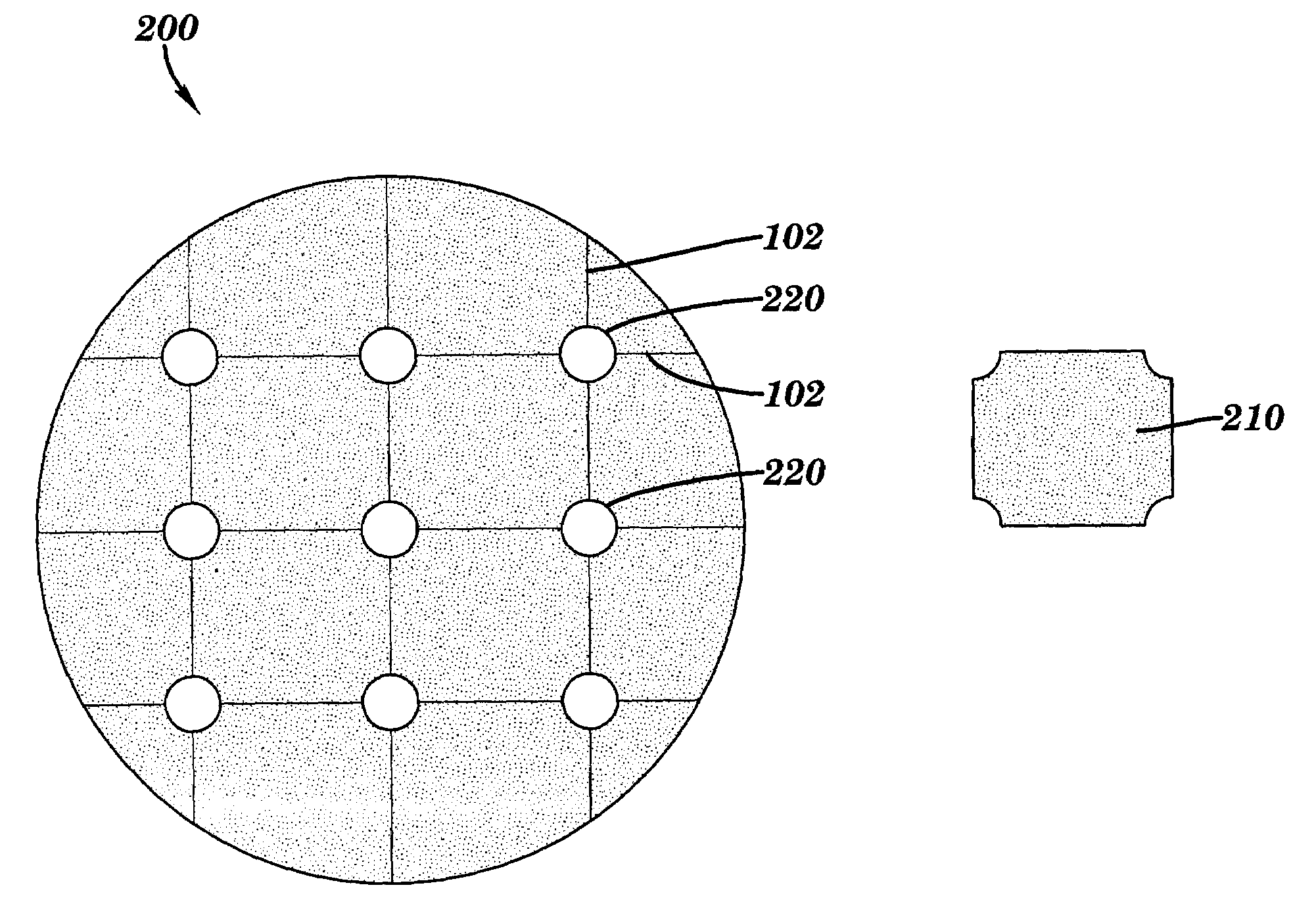
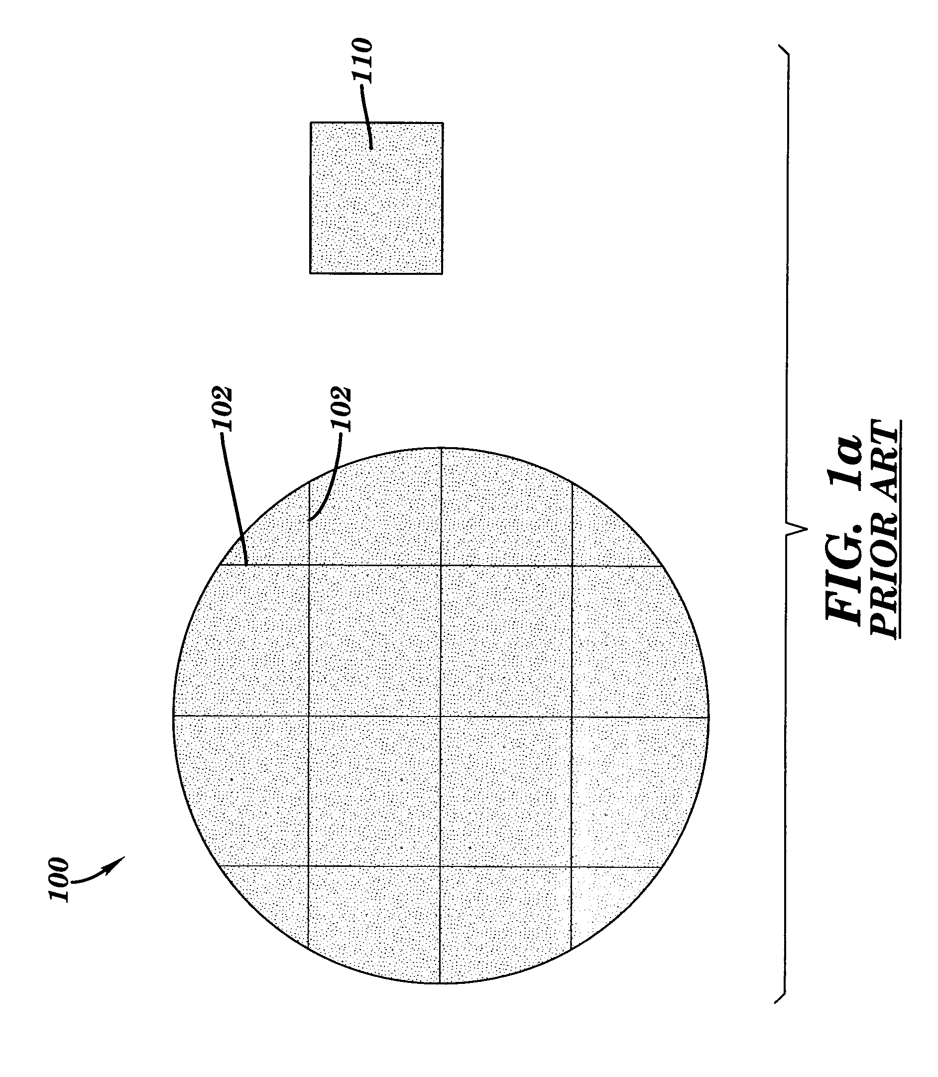
[0021]By way of overview and introduction, the invention is directed to a method for creating a semiconductor chip absent any ninety degree angles. The semiconductor chip originates from a semiconductor wafer with dicing channels that separate semiconductor chips and holes at each intersection of the dicing channels. Once diced, semiconductor chips are created without any ninety degree angles.

[0022]An embodiment of the invention 200 will be described with reference to the FIG. 2a. As shown the semiconductor wafer 200 includes holes 220 at the intersection of the dicing channels 102. The holes 220 can be created by laser drilling, Bosch process deep drilling, photolithography followed by reactive ion etching, or ion milling. ...


PUM


Abstract

The invention is directed to an improved semiconductor chip that reduces crack initiation and propagation into the active area of a semiconductor chip. A semiconductor wafer includes dicing channels that separate semiconductor chips and holes through a portion of a semiconductor chip, which are located at the intersection of the dicing channels. Once diced from the semiconductor wafer, semiconductor chips are created without ninety degree angle corners.

Description

BACKGROUND OF THE INVENTION[0001]1. Field of the Invention[0002]The invention relates generally to semiconductor devices, and more particularly to a semiconductor chip shape alteration.[0003]2. Description of the Related Art[0004]The shape of a semiconductor chip is important to semiconductor technology. The shape of a semiconductor chip can cause physical stress on the semiconductor chip. Stress on the semiconductor chip causes delamination, which is the fracture of a semiconductor chip's Back End of the Line (“BEOL”) materials, which in turn leads to semiconductor chip failure. Prior art semiconductor chips are limited to square and rectangular shapes, which introduce the most stress on the semiconductor chip, because of the ninety degree corners inherent in such shapes.[0005]FIGS. 1a-1b depict a prior art semiconductor wafer 100 and chip 110. Note the perpendicular dicing channels 102 in the prior art semiconductor wafer 100. Once diced, singulated die, also known as semiconducto...

Claims


Application Information

Patent Timeline
Patent Type & Authority Patents(United States)
IPC IPC(8): H01L21/78
CPCH01L21/67092H01L21/78H01L23/562H01L29/0657H01L2924/0002H01L2924/00H01L23/48
Inventor FAROOQ, MUKTA G.JUNG, DAE-YOUNGMELVILLE, IAN D.
Owner GLOBALFOUNDRIES INC
Why Eureka
Try Eureka