Read-only memory

a read-only memory and memory cell technology, applied in the field of read-only memory, can solve the problems of increasing the bulk, coupling between neighboring bit lines in the array, and reducing the density of the structure, and achieve the effect of reducing the physical stress

Inactive Publication Date: 2008-11-04
STMICROELECTRONICS SRL
View PDF15 Cites 6 Cited by
  • Summary
  • Abstract
  • Description
  • Claims
  • Application Information

AI Technical Summary

Benefits of technology

[0021]One embodiment of the present invention decreases the physical stress linked to the isolating trenches of the structure.

Problems solved by technology

A problem of ROM cell arrays is linked to electromigration on the ground lines due to the significant number of cells likely to discharge the precharge current.
The intensity of the current to be conveyed by these grounded lines results either in oversizing said lines, and thus increasing the bulk, or in limiting the number of cells addressable in parallel in the memory plane, and thus the density.
Another disadvantage of ROM cells is due to the coupling between neighboring bit lines in the array.
This problem is more and more critical as memory cell arrays miniaturize and generates read errors.
Such a solution has the disadvantage of decreasing the density of the structure.
Further, it does not solve the problem of electromigration on ground conductors.
Another problem of known ROM architectures is due to the presence of shallow isolation trenches (STI) in the integrated structure to separate the transistors forming the cells.
The size of such isolation trenches generates a physical stress on the transistors.
This problem results in increasing the respective transistor sizes.

Method used


Image

  • Read-only memory
  • Read-only memory
  • Read-only memory

Examples


Embodiment Construction

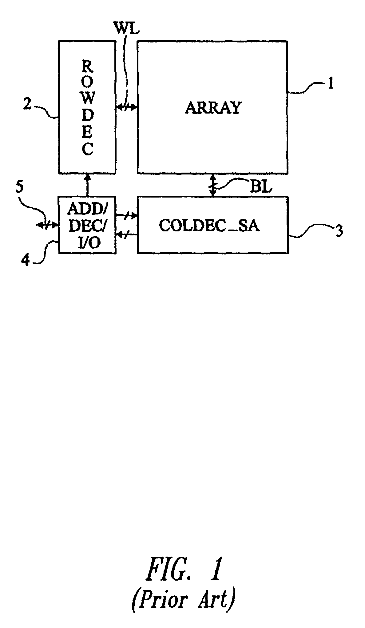
[0035]Same elements have been designated with same reference numerals in the different drawings. For clarity, only those elements useful to the understanding of the present invention have been shown in the drawings and will be described hereafter. In particular, the circuits for reading and addressing the memory cells of an array according to the present invention have not been discussed.

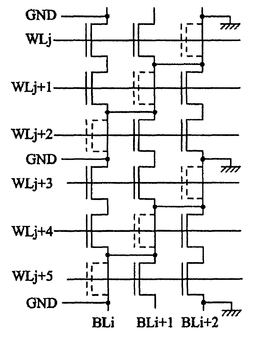
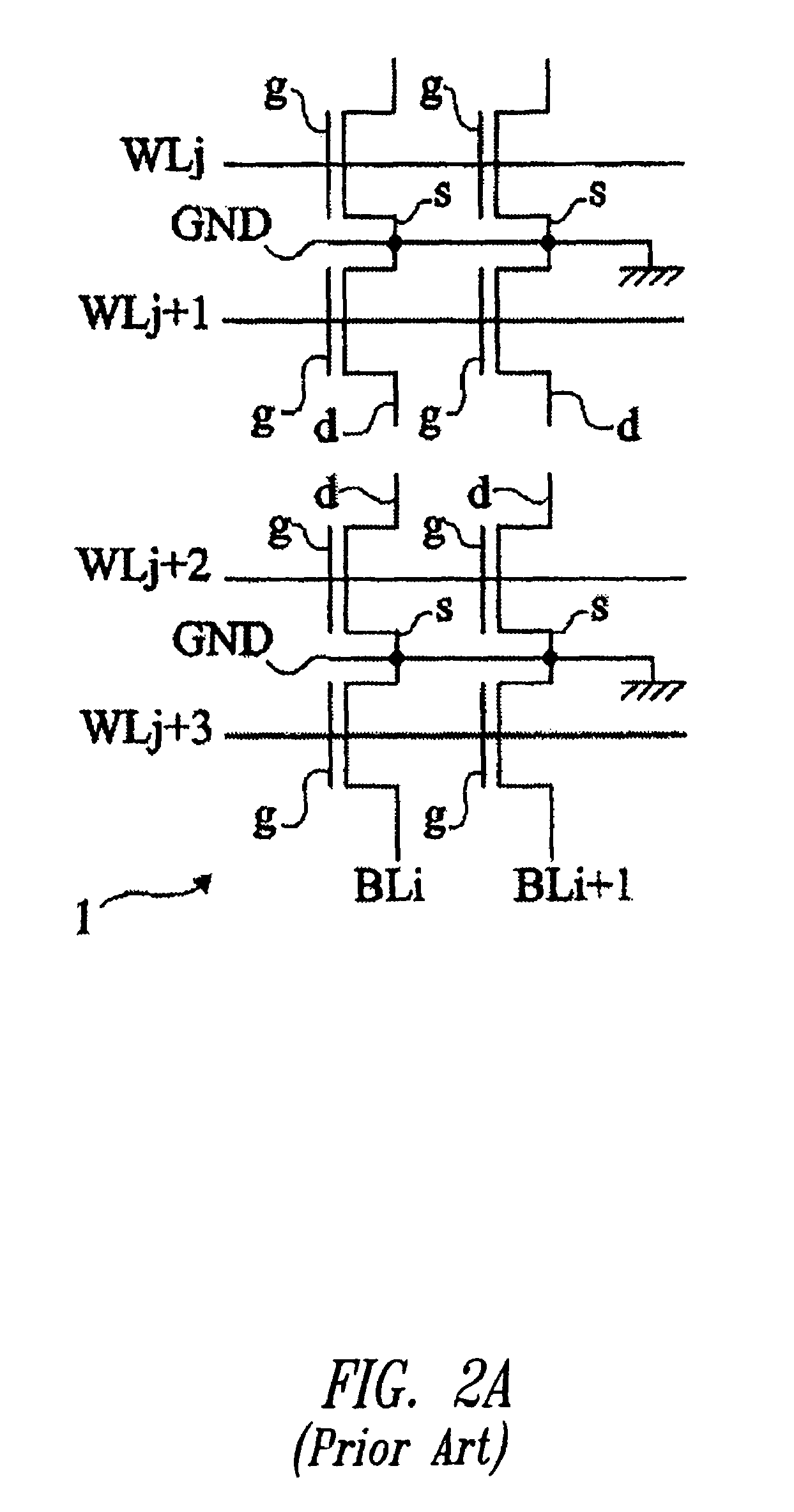
[0036]FIGS. 4A and 4B very schematically show an embodiment of a ROM cell array according to the present invention. These drawings should be compared with previously-described FIGS. 2A and 2B, and respectively illustrate the equivalent electric diagram of the memory cell array and a simplified top view of the corresponding integrated circuit.

[0037]As previously, each cell is formed of a MOS transistor (for example, with an N channel) having its programmed or not state depending on the transfer of a contact from a drain or source region to a conductive line (bit line) to condition the discharge to gr...


PUM


Abstract

An array of ROM cells, each formed of a transistor having a first drain or source region connected to a bit line connecting several transistors in a first direction, the gates of the different transistors being connected to word lines in a second direction perpendicular to the first one, the array comprising a repetition of an elementary pattern extending over three lines in each direction and comprising nine transistors arranged so that each of the lines of the elementary pattern comprises two cells, two neighboring transistors of each pattern in the first direction sharing a same second region connected to a ground line and being connected to different bit lines from a word line to the other.

Description

BACKGROUND OF THE INVENTION[0001]1. Field of the Invention[0002]The present invention generally relates to read only memories (ROM) having the respective states of the cells are set on manufacturing of the integrated circuit containing the memory. The present invention more specifically relates to the forming of an array of memory cells formed of MOS transistors. It applies whether the programming of each cell is performed by the taking of a contact on one of the source or drain regions of the transistor (memory generally known as a “ROM contact”), or it is performed by the forming of a conductive via from a source or drain contact area to a metal track conveying the signals (memory generally known as a “ROM via”).[0003]2. Description of the Related Art[0004]FIG. 1 very schematically shows in the form of blocks an example of a ROM of the type to which the present invention applies. Such a structure is intended to be made in integrated form, possibly with other components.[0005]A ROM...

Claims


Application Information

Patent Timeline
Patent Type & Authority Patents(United States)
IPC IPC(8): G11C11/34
CPCG11C7/18G11C17/12H01L27/112H10B20/00
Inventor JACQUET, FRANCOIS
Owner STMICROELECTRONICS SRL
Why Eureka
Try Eureka