Check patentability & draft patents in minutes with Patsnap Eureka AI!

ESD protection circuit with active triggering

a protection circuit and active triggering technology, applied in the direction of transistors, semiconductor devices, electrical apparatus, etc., can solve the problem that devices are more vulnerable to electrostatic discharg

Active Publication Date: 2010-02-02
AMAZING MICROELECTRONICS
View PDF11 Cites 10 Cited by
  • Summary
  • Abstract
  • Description
  • Claims
  • Application Information

AI Technical Summary

Benefits of technology

These circuits effectively protect ICs from ESD damage by triggering appropriate discharging paths during ESD events, reducing coupling effects and enhancing protection across all ESD modes, including PD-mode, PS-mode, ND-mode, and NS-mode, while maintaining normal operation during non-ESD conditions.

Problems solved by technology

As the scale of devices in ICs has become smaller, the devices have become more vulnerable to Electrostatic discharge (ESD).
Hence, ESD has been one of the most important reliability issues for IC products and must be taken into consideration in the design phase of all ICs.

Method used


Image

  • ESD protection circuit with active triggering
  • ESD protection circuit with active triggering
  • ESD protection circuit with active triggering

Examples


first embodiment

[0043]Please refer to FIG. 7, which illustrates the ESD protection circuit in the first embodiment according to the invention. This ESD protection circuit 70 includes a discharging component 72, a diode D1, and an ESD detection circuit 74. The discharging component 72 is coupled between an input / output pad and a first power line (VSS) of the IC in which the ESD protection circuit 70 is set. The diode D1 is coupled between the input / output pad and a second power line (VDD) of the IC in a forward direction toward the second power line.

[0044]The ESD detection circuit 74 includes a resistor R1, a capacitor C1, and a triggering component. In this embodiment, the triggering component is an inverter labeled as INV_1. The resistor R1 and the capacitor C1 are formed in series and coupled between the first power line and the second power line. As shown in FIG. 7, the inverter INV_1 has a positive power end coupled to the input / output pad and a negative power end coupled to the first power lin...

second embodiment

[0048]Please refer to FIG. 8, which illustrates the ESD protection circuit in the second embodiment according to the invention. This ESD protection circuit 80 includes a discharging component 82, a diode, and an ESD detection circuit 84. The discharging component 82 is coupled between an input / output pad and a first power line (VDD) of an IC. The diode is coupled between the input / output pad and a second power line (VSS) of the IC in a forward direction toward the input / output pad.

[0049]The ESD detection circuit 84 includes a capacitor C1, a resistor R1, and a triggering component. In this embodiment, the triggering component is composed of two inverters, INV_2 and INV_3, coupled in series. The capacitor C1 and resistor R1 are formed in series between the first power line and the second power line. As shown in FIG. 8, the inverters respectively have a positive power end coupled to the first power line and a negative power end coupled to the input / output pad. Besides, the input of th...

third embodiment

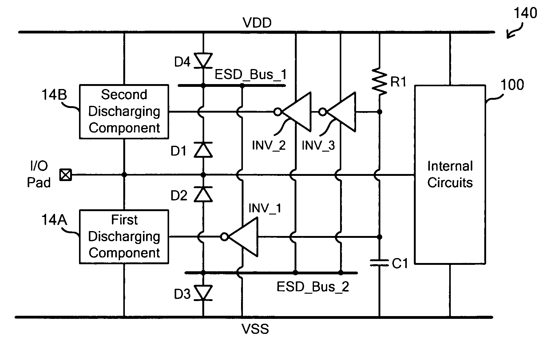
[0053]Please refer to FIG. 11, which illustrates the ESD protection circuit in the third embodiment according to the invention. In this embodiment, the circuits in FIG. 7 and FIG. 8 are combined to cope with all ESD conditions (PD-mode, PS-mode, ND-mode, and NS-mode).

[0054]As shown in FIG. 11, the ESD protection circuit 110 includes a first discharging component 92, a second discharging component 94, and an ESD detection circuit 96. The first discharging component 92 is coupled between an input / output pad and a first power line (VSS) of an IC. The second discharging component 94 is coupled between the input / output pad and a second power line (VDD) of the IC.

[0055]The ESD detection circuit 96 includes a capacitor C1, a resistor R1, and three inverters. The first inverter INV_1 has a first positive power end coupled to the input / output pad and a first negative power end coupled to the first power line. The input of the first inverter INV_1 is coupled to the node between the capacitor ...


PUM


Abstract

An ESD protection circuit is provided. The circuit includes a discharging component, a diode, and an ESD detection circuit. The discharging component is coupled between an input / output pad and a first power line of an IC. The diode is coupled between the input / output pad and a second power line of the IC in a forward direction toward the second power line. The ESD detection circuit includes a capacitor, a resistor, and a triggering component. The capacitor and the resistor are formed in series and coupled between the first power line and the second power line. The triggering component has a positive power end coupled to the input / output pad and a negative power end coupled to the first power line. An input of the triggering component is coupled to a node between the capacitor and the resistor.

Description

BACKGROUND OF THE INVENTION[0001]1. Field of the Invention[0002]The present invention relates to an electrostatic discharge (ESD) protection circuit. In particular, the present invention relates to an ESD protection circuit suitable for applying in an integrated circuit (IC).[0003]2. Description of the Prior Art[0004]As the scale of devices in ICs has become smaller, the devices have become more vulnerable to Electrostatic discharge (ESD). Hence, ESD has been one of the most important reliability issues for IC products and must be taken into consideration in the design phase of all ICs.[0005]Besides an ESD clamp device, an ESD detection circuit is another critical component in on-chip ESD protection circuits because it highly relates to the ESD protection capability of an on-chip ESD protection circuit. The ESD detection circuit is designed to provide trigger currents to turn on the ESD clamp device when the IC product is under ESD stresses.[0006]A variety of ESD detection circuits ...

Claims


Application Information

Patent Timeline
Patent Type & Authority Patents(United States)
IPC IPC(8): H02H9/00
CPCH01L27/0266H01L2924/0002H01L2924/00
Inventor KER, MING-DOUHSIAO, YUAN-WENJIANG, RYAN HSIN-CHIN
Owner AMAZING MICROELECTRONICS
Features
  • R&D
  • Intellectual Property
  • Life Sciences
  • Materials
  • Tech Scout
  • Unparalleled Data Quality
  • Higher Quality Content
  • 60% Fewer Hallucinations
Learn More