

Chip resistor and manufacturing method thereof
a technology of chip resistor and manufacturing method, which is applied in the manufacture of resistor chips, resistor details, resistive material coating, etc., can solve the problems of increasing production costs and low circuit board productivity, and achieve the effect of efficiently and appropriately making such a chip resistor
- Summary
- Abstract
- Description
- Claims
- Application Information
AI Technical Summary
Benefits of technology
Problems solved by technology
Method used
Image

Examples
first embodiment
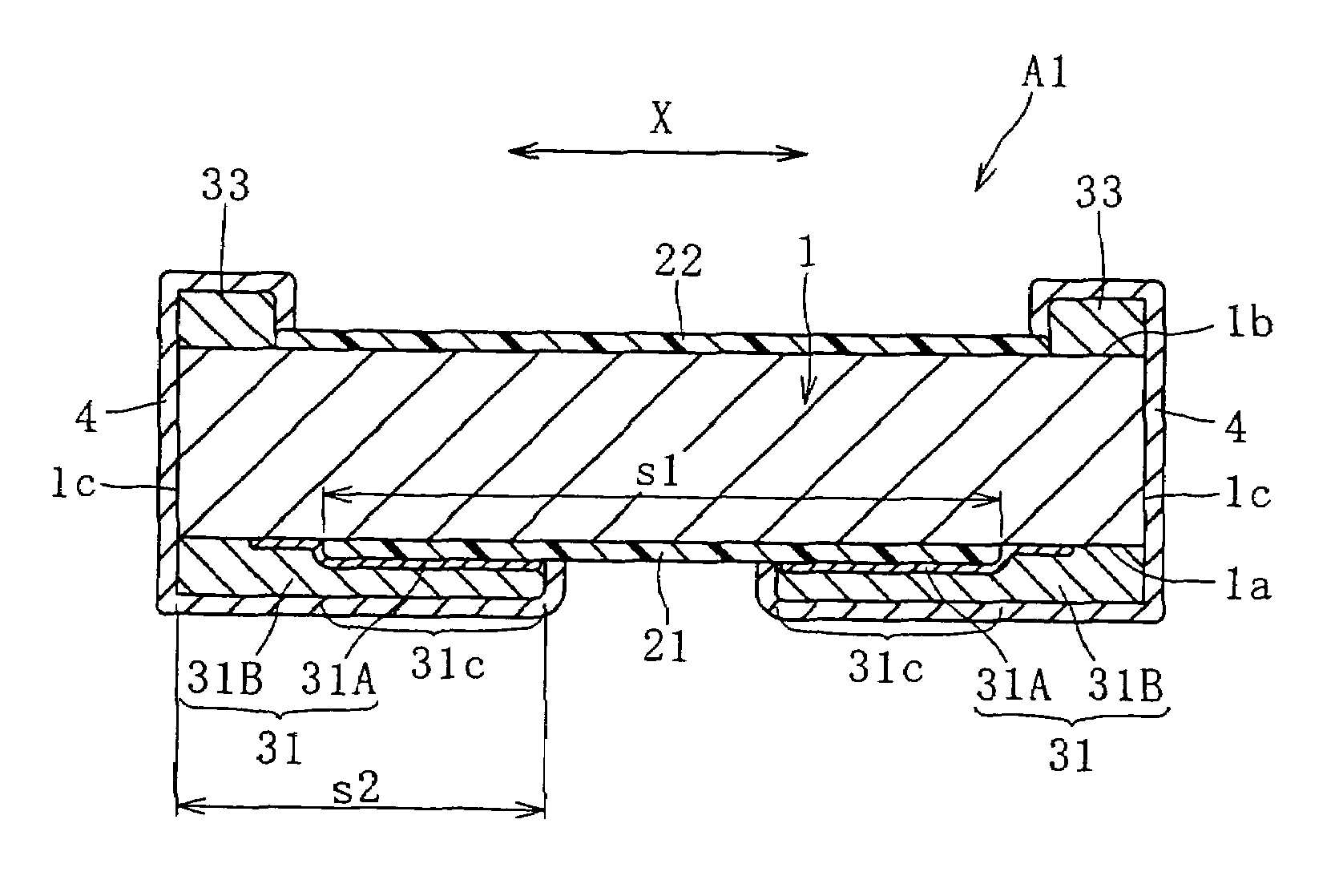
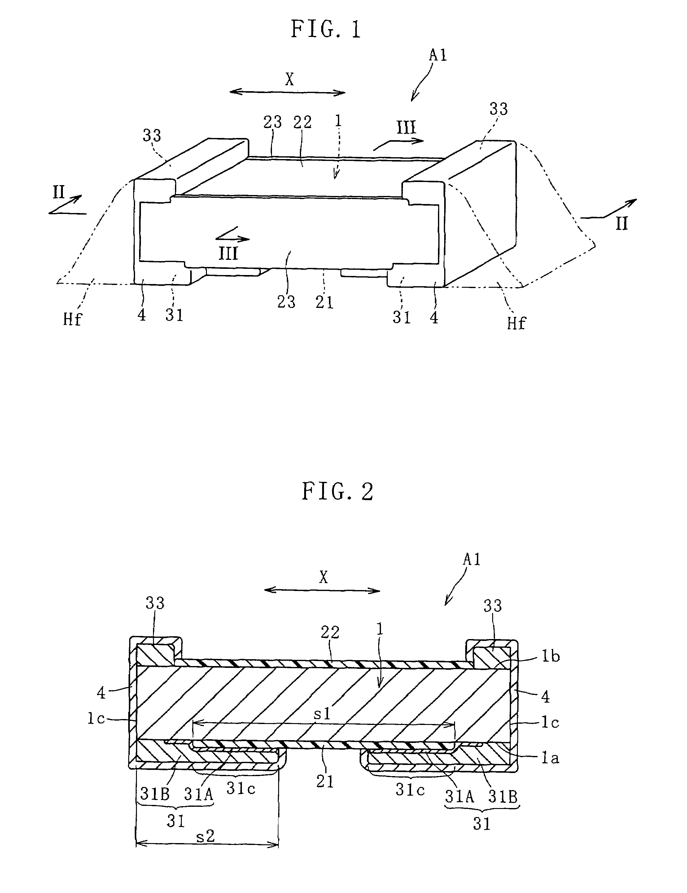
[0036]FIG. 1 through FIG. 4 show a chip resistor according to the present invention. The chip resistor A1 includes a resistor element 1, insulation films 21-23, a pair of lower electrodes 31, a pair of upper electrodes (auxiliary electrodes) 33, and a pair of plated layers 4 (not illustrated in FIG. 4) to facilitate soldering. The chip resistor A1 has a low resistance of 0.5 mΩ˜100 mΩ for example. It should be noted, however, that this range of resistance is nothing more than an example, and the scope of the present invention is not limited to resistors which have such a low resistance.
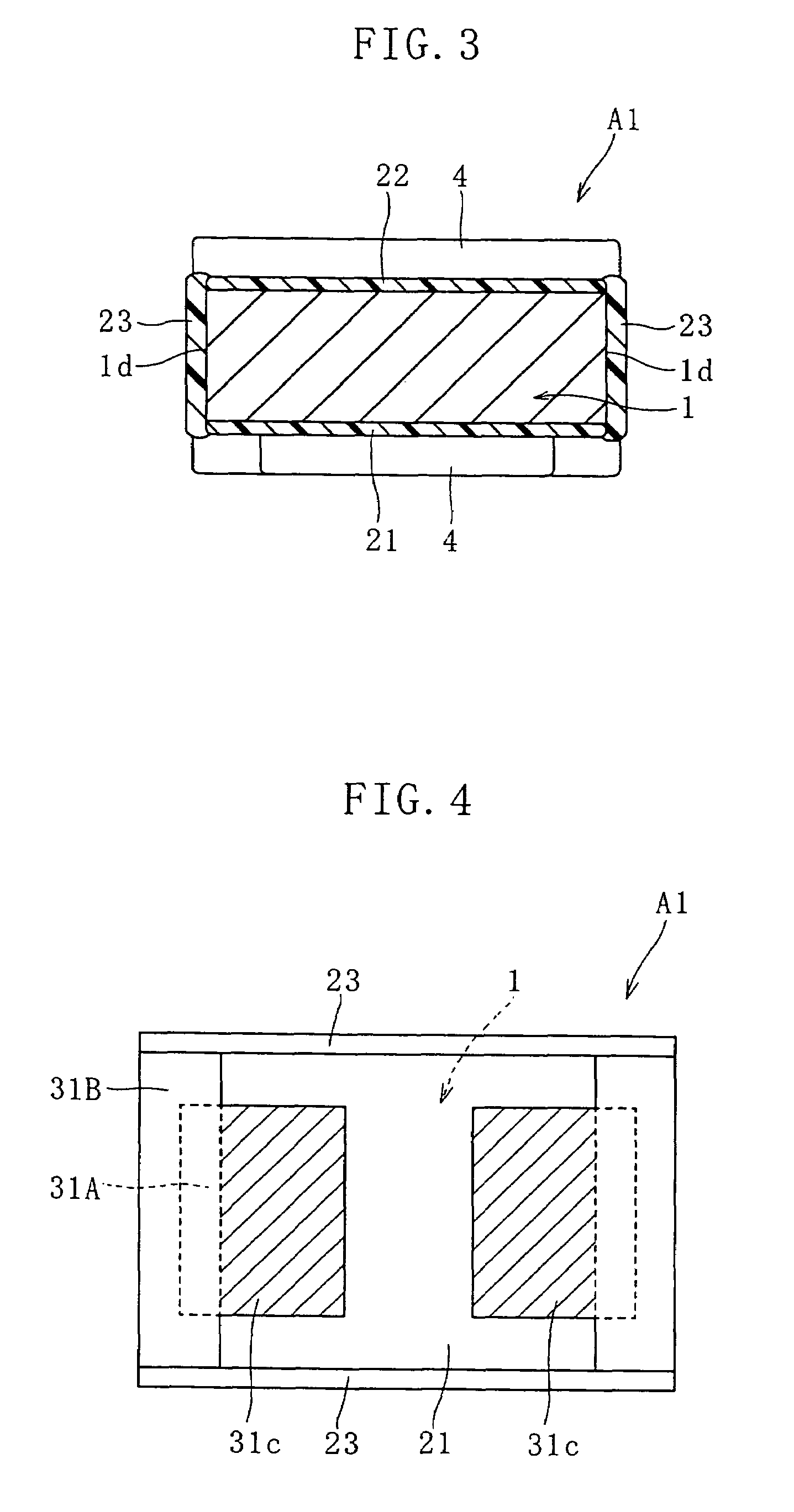
[0037]The resistor element 1 is a chip which has a uniform thickness and a rectangular plan view, and as shown in FIG. 2 or FIG. 3, has a bottom surface 1a, an upper surface 1b, two end surfaces 1c (spaced from each other in the direction X) and two side surfaces 1d (longitudinal in the direction X). The resistor element 1 is made of a Ni—Cu alloy or a Cu—Mn alloy for example. It should be noted that ...
embodiment 1
[0065]Then, an insulation film 23 is formed on all the side surfaces 11d of each bar 11. The insulation film 23 is made of the same material as that used for making the insulation layer 21A and the insulation film 22. The insulation film 23 may be formed by the same method as used in the formation of the insulation film 23 in the
[0066]Next, as shown in FIGS. 12A and 12B, plural pieces of a conductive layer 31B′ and a plural pieces of a conductive layer 33′ are formed (each indicated by cross-hatching) on the first surface 11a and the second surface 11b of each bar 11 where the insulation layer 21A and the insulation film 22 are not present. Each region on the first surface 11a covered by the conductive layer 32′ will provide a lower electrode 32 and each region on the second surface 11b covered by the conductive layer 33′ will provide an auxiliary electrode 33. The conductive layers 32′, 33′ may be formed by copper plating for example.
[0067]As shown in FIG. 13A, plural pieces of a s...
third embodiment
[0070]FIGS. 14A and 14B show a chip resistor A3 according to the present invention. As shown in FIG. 14B, the chip resistor A3 is provided with four electrodes 32B on a bottom surface 1a of a resistor element 1. These electrodes 32B are formed by first forming a cross-shaped insulation layer 21A on the bottom surface 1a of the resistor element 1 and then plating the bottom surface 1a. Thereafter, by forming a second insulation layer 21B, the chip resistor A3 is obtained. It should be appreciated that the figure does not show plated layers which is formed to facilitate soldering, for convenience of description.
[0071]The chip resistor A3 has four electrodes 32B, and can be utilized in the following way. Supposing that the resistance of the chip resistor A3 is given, two of the four electrodes 32B are used for supplying electric current, and the other two electrodes 32B are used for voltage measurement. The pair of current application electrodes are connected to the circuit so as to al...
PUM
| Property | Measurement | Unit |
|---|---|---|
| resistance | aaaaa | aaaaa |
| thickness | aaaaa | aaaaa |
| thickness | aaaaa | aaaaa |
Abstract
Description
Claims
Application Information