
Routing signals to drivers of display device with minimized wiring

a technology of display device and driver, applied in static indicating devices, non-linear optics, instruments, etc., can solve the problems of increasing power consumption and emi (electromagnetic interference), increasing power consumption and emi (electromagnetic interference) during transmission of such rgb color data, etc., to minimize wiring and minimize power consumption and emi.

Inactive Publication Date: 2010-04-20
SAMSUNG ELECTRONICS CO LTD
View PDF4 Cites 0 Cited by
  • Summary
  • Abstract
  • Description
  • Claims
  • Application Information

AI Technical Summary

Benefits of technology

[0020]In this manner, data signals are transmitted to the line drivers of the display panel from the timing controller with minimized wiring. Such minimized wiring is advantageous for in turn minimizing power consumption and EMI (electromagnetic interference), especially for large display panels having a large number of line drivers.

Problems solved by technology

Such signal transmission through such increased wiring results in increased power consumption and EMI (electromagnetic interference).
Such increased wiring in turn disadvantageously increases power consumption and EMI (electromagnetic interference) during transmission of such RGB color data.

Method used


Image

  • Routing signals to drivers of display device with minimized wiring
  • Routing signals to drivers of display device with minimized wiring
  • Routing signals to drivers of display device with minimized wiring

Examples


Embodiment Construction

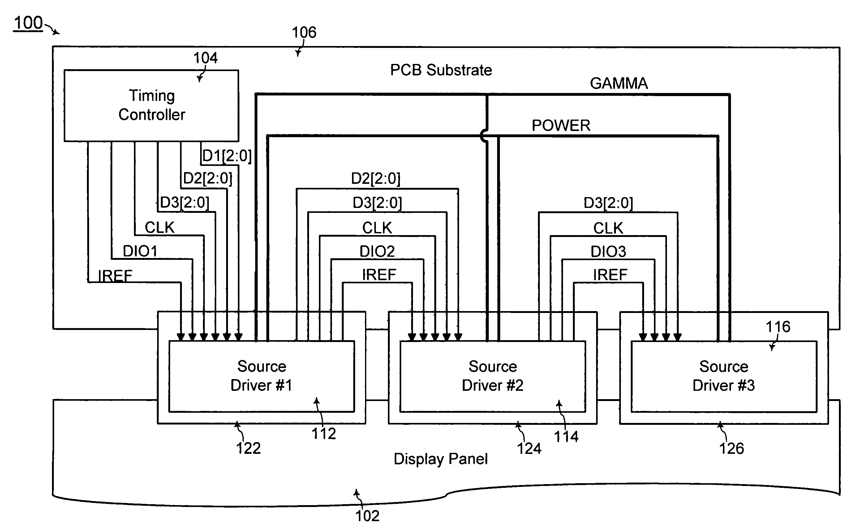
[0030]FIG. 3 shows a block diagram of a display device 100 with minimized signal wiring according to an embodiment of the present invention. The display device includes a display panel 102 and also includes a timing controller 104 mounted on a PCB (printed circuit board) substrate 106. The display device additionally includes a plurality of source drivers including a first source driver 112, a second source driver 114, and a third source driver 116.

[0031]Each of the source drivers 112, 114, and 116 are disposed on a respective film 122, 124, and 126. The films 122, 124, and 126 are comprised of a filler material to interface the source drivers 112, 114, and 116 between the PCB substrate 106 and the display panel 102. Such filler material is individually known to one of ordinary skill in the art.

[0032]Further in FIG. 3, a GAMMA voltage which is a reference voltage used by a respective DAC (digital to analog converter) within each of the source drivers 112, 114, and 116 is coupled to ...


PUM


Abstract

A display device includes a first set of data buses coupled between a timing controller and a first line driver. In addition, the display device also includes a second set of at least one data bus coupled between the first line driver and a second line driver. The second set has a less number of at least one data bus than the first set. Thus, data signals are transmitted to the line drivers of the display panel from the timing controller with minimized wiring for reduced power consumption and electromagnetic interference.

Description

CROSS-REFERENCE TO RELATED APPLICATION(S)[0001]The present application claims priority under 35 U.S.C. § 119 to Korean Patent Application No. 2004-99723, filed on Dec. 1, 2004, which is incorporated herein by reference in its entirety.TECHNICAL FIELD[0002]The present invention relates generally to display devices such as LCD (liquid crystal display) panels, and more particularly, to minimizing signal wiring to drivers in a display device with a large display panel for in turn minimizing EMI (electromagnetic interference) and power consumption.BACKGROUND OF THE INVENTION[0003]FIG. 1 shows a block diagram of components of a display device 10 such as a TFT-LCD (thin film transistor liquid crystal display) device. The display device 10 includes a display panel 12, a source driver block 14, a gate driver 16, a timing controller 18, and a power source 20.[0004]The display panel 12 includes a plurality of source (i.e., data) lines S1, S2, . . . , and so on to SN. The display panel 12 also ...

Claims


Application Information

Patent Timeline
Patent Type & Authority Patents(United States)
IPC IPC(8): G09G3/36
CPCG09G3/20G09G3/3611G09G2370/08G09G2310/027G09G2352/00G09G2300/0426G09G3/30G09G3/36G02F1/133
Inventor KIM, KYUNG-WOLJEON, YONG-WEON
Owner SAMSUNG ELECTRONICS CO LTD
Features
  • Generate Ideas
  • Intellectual Property
  • Life Sciences
  • Materials
  • Tech Scout
  • Unparalleled Data Quality
  • Higher Quality Content
  • 60% Fewer Hallucinations
Learn More