Pixel circuit, display device, and method for driving pixel circuit

a pixel circuit and display device technology, applied in the direction of electric variable regulation, process and machine control, instruments, etc., can solve the problems of i-v characteristic deterioration along with elapse, difficult to realize a large-scale and high-definition display, and considered extremely difficult with the current level of technology, so as to achieve no luminance deterioration

Inactive Publication Date: 2010-05-11
SONY CORP
View PDF14 Cites 66 Cited by
  • Summary
  • Abstract
  • Description
  • Claims
  • Application Information

AI Technical Summary

Benefits of technology

[0043]An object of the present invention is to provide a pixel circuit, display device, and method of driving a pixel circuit enabling source-follower output with no deterioration of luminance even with a change of the current-voltage characteristic of the light emitting element along with elapse, enabling a source-follower circuit of n-channel transistors, and able to use an n-channel transistor as a drive element of an electro-optic element while using current anode-cathode electrodes.

Problems solved by technology

While the former has a simple structure, it has the problem that realization of a large sized and high definition display is difficult.
However, here too, similarly, the I-V characteristic of the EL element ends up deteriorating along with elapse.
This is considered extremely difficult with the current level of technology.

Method used


Image

  • Pixel circuit, display device, and method for driving pixel circuit
  • Pixel circuit, display device, and method for driving pixel circuit
  • Pixel circuit, display device, and method for driving pixel circuit

Examples


first embodiment

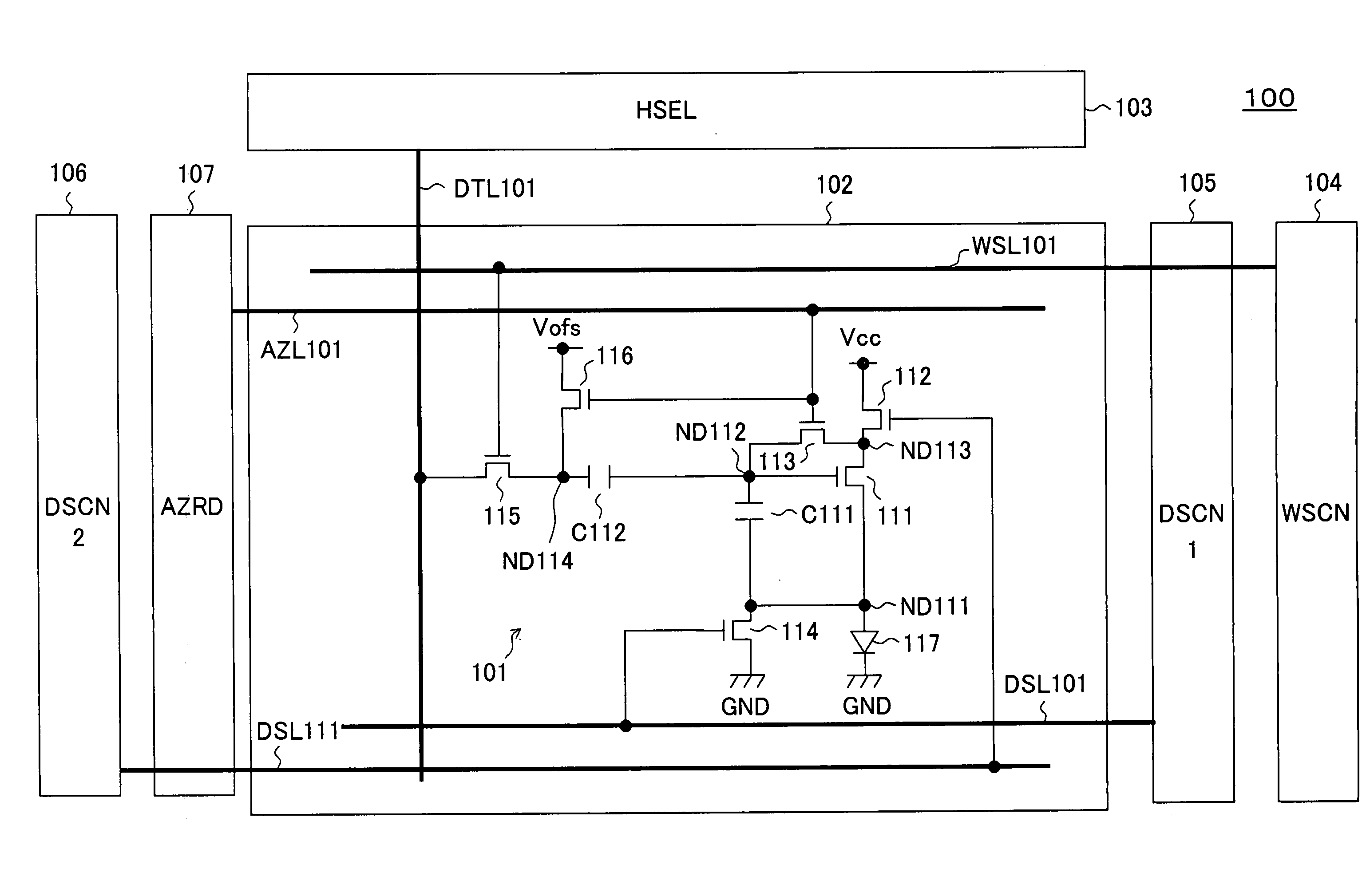
[0110]FIG. 8 is a block diagram of the configuration of an organic EL display device employing pixel circuits according to the first embodiment.

[0111]FIG. 9 is a circuit diagram of the concrete configuration of a pixel circuit according to the first embodiment in the organic EL display device of FIG. 8.

[0112]This display device 100 has, as shown in FIG. 8 and FIG. 9, a pixel array portion 102 having pixel circuits (PXLC) 101 arranged in an m×n matrix, a horizontal selector (HSEL) 103, a write scanner (WSCN) 104, a first drive scanner (DSCN1) 105, a second drive scanner (DSCN2) 106, an auto zero circuit (AZRD) 107, data lines DTL101 to DTL10n selected by the horizontal selector 103 and supplied with a data signal in accordance with the luminance information, scanning lines WSL101 to WSL10m selectively driven by the write scanner 104, drive lines DSL101 to DSL10m selectively driven by the first drive scanner 105, drive lines DSL111 to DSL11m selectively driven by the second drive scan...

second embodiment

[0204]FIG. 23 is a block diagram of the configuration of an organic EL display device employing pixel circuits according to a second embodiment.

[0205]FIG. 24 is a circuit diagram of the concrete configuration of a pixel circuit according to the second embodiment in the organic EL display device of FIG. 23.

[0206]The difference of the second embodiment from the above first embodiment is that a single drive scanner is used, the drive signal ds[1] applied to the drive lines DSL101 to DSL10m is supplied to the gate of the TFT 114, and the inverted signal / ds[1] of the drive signal ds[1] due to the inverters 108-1 to 108-m is supplied to the gate of the TFT 112.

[0207]Therefore, in the second embodiment, the TFT 112 and TFT 114 are complementarily turned on and off. That is, when the TFT 112 is on, the TFT 114 is held off, while when the TFT 112 is off, the TFT 114 is held on.

[0208]The operation of the second embodiment will be explained with reference to FIG. 25A to FIG. 25D, FIGS. 26A and...

third embodiment

[0233]FIG. 29 is a block diagram of the configuration of an organic EL display device employing pixel circuits according to a third embodiment.

[0234]FIG. 30 is a circuit diagram of the concrete configuration of a pixel circuit according to the third embodiment in the organic EL display device of FIG. 20.

[0235]The difference of the display device 100B according to the third embodiment from the display device 100A according to the second embodiment lies in the use of the p-channel TFT 112B instead of the n-channel TFT for the TFT 112 as the first switch in the pixel circuit.

[0236]In this case, the TFT 112B and TFT 114 need only be complementarily turned on and off, so as shown in FIG. 31A to FIG. 31C, it is sufficient to apply only the drive signal ds[1] to one drive line DSL101 to DSL10m of each row.

[0237]Therefore, like in the second embodiment, there is no need to provide an inverter.

[0238]The rest of the configuration is similar to above second embodiment.

[0239]According to the th...


PUM


Abstract

A pixel circuit, display device, and method of driving a pixel circuit enabling source-follower output with no deterioration of luminance even with a change of the current-voltage characteristic of the light emitting element along with elapse, enabling a source-follower circuit of n-channel transistors, and able to use an n-channel transistor as a drive transistor of a light emitting element while using current anode-cathode electrodes, wherein a capacitor C111 is connected between a gate and source of a TFT 111 as a drive transistor, a source side of the TFT 111 is connected to a fixed potential (for example GND) through the TFT 114, the gate and drain of the TFT 111 are connected through the TFT 113 to cancel the threshold value Vth, the threshold value Vth is charged in the capacitor C111, and the input voltage Vin is coupled with the gate of the TFT 111 from the threshold voltage Vth.

Description

TECHNICAL FIELD[0001]The present invention relates to a pixel circuit having an electro-optic element with a luminance controlled by a current value in an organic EL (electroluminescence) display etc., an image display device comprised of such pixel circuits arrayed in a matrix, in particular a so-called active matrix type image display device controlled in value of current flowing through the electro-optic elements by insulating gate type field effect transistors provided inside the pixel circuits, and a method of driving a pixel circuit.BACKGROUND ART[0002]In an image display device, for example, a liquid crystal display, a large number of pixels are arranged in a matrix and the light intensity is controlled for every pixel in accordance with the image information to be displayed so as to display an image.[0003]This same is true for an organic EL display etc. An organic EL display is a so-called self-light emitting type display having a light emitting element in each pixel circuit...

Claims


Application Information

Patent Timeline
Patent Type & Authority Patents(United States)
IPC IPC(8): G09G3/30G09G3/20H01L51/50G09G3/32
CPCG09G3/3233G09G2300/0819G09G2320/043G09G2300/0861G09G2310/0256G09G2300/0852G09G3/30G09G3/20
Inventor UCHINO, KATSUHIDEYAMASHITA, JUNICHIYAMAMOTO, TETSURO
Owner SONY CORP
Why Eureka
Try Eureka