
Power supply

a power supply and power supply technology, applied in the field of power supplies, can solve problems such as system down, memory operation error, and tendency to increase output voltage, and achieve the effect of preventing the occurrence of voltage increase and preventing abnormal oscillation

Inactive Publication Date: 2010-05-25
FDK CORP
View PDF11 Cites 3 Cited by
  • Summary
  • Abstract
  • Description
  • Claims
  • Application Information

AI Technical Summary

Benefits of technology

[0050]Accordingly, it is a general object of the present invention to provide a power supply in which the above-described disadvantage is eliminated.
[0055]On the other hand, according to one aspect of the present invention, a non-directional impedance element is inserted between the differential input terminals of a differential amplifier (or a load current comparison part), so that the above-described problem is solved and it is possible to prevent occurrence of the problem of voltage increase.
[0056]Thus, according to one aspect of the present invention, in a power supply, a non-directional impedance element is inserted between the differential input terminals of a differential amplifier (or a load current comparison part), so that the differential output value of the differential amplifier is prevented from increasing more than necessary even when a maximum load current value is higher than its own load current value of the power supply. As a result, by providing a capacitor for high frequency removal, it is possible to prevent abnormal oscillation. Further, it is possible to provide a power supply that can ensure prevention of occurrence of the above-described problem of voltage increase even when a directional impedance element for cutting off a signal indicating the load current value of the power supply when it is lower than the maximum load current value is provided.

Problems solved by technology

This sharp variation in the output current affects a current balance circuit of Highest Current Mode, so that the problem of increasing output voltage tends to occur.
In particular, this problem is prominent in a DDC for memory, in which a sharp variation is periodically caused in load current, so that there is the possibility of occurrence of memory operation error and, further, system down due to activation of the overvoltage protection circuit of the DDC.
Further, in the current balance circuit of the highest current mode, periodic variations in load current may cause an increase in output voltage.
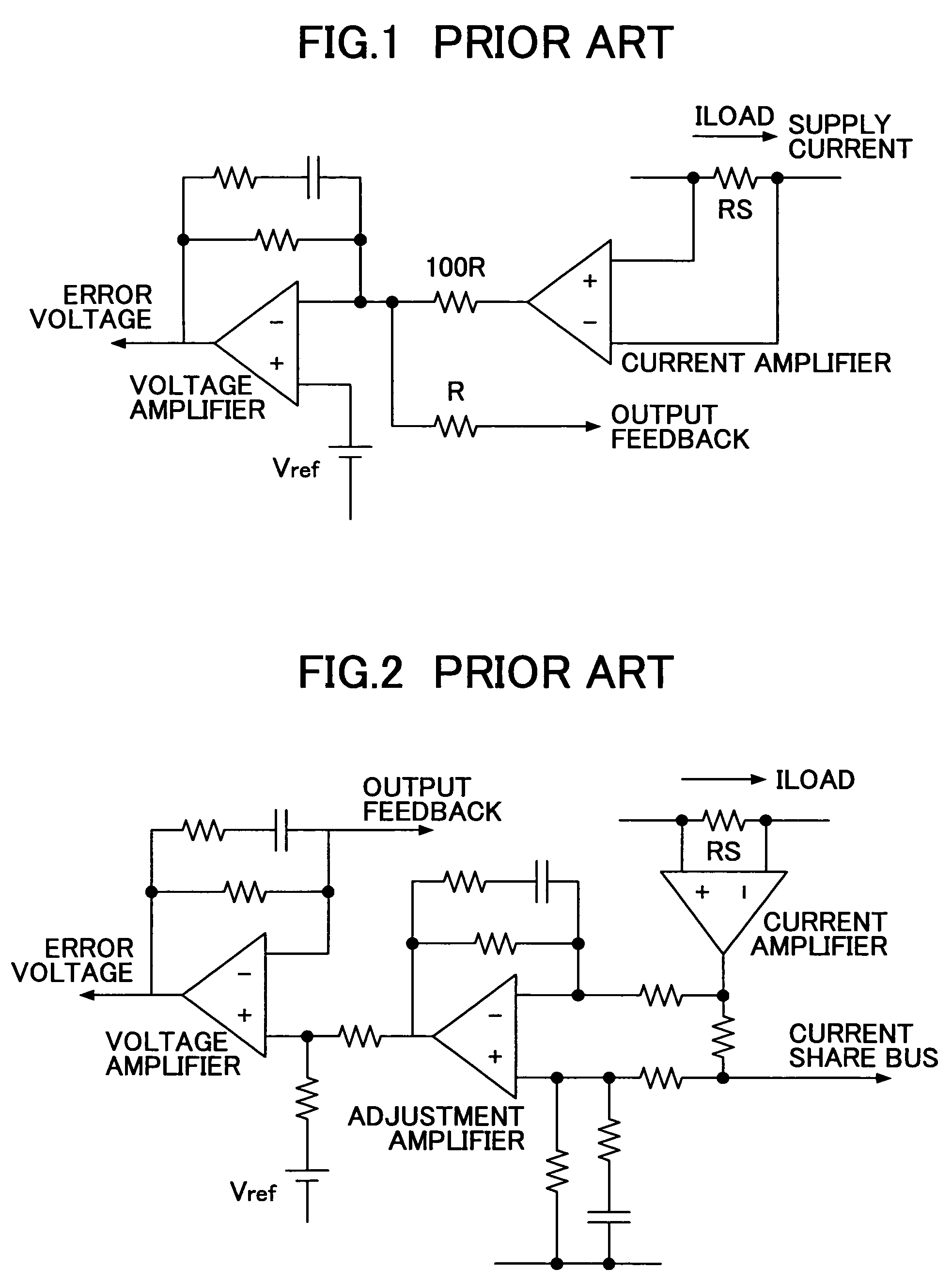
This mode has a circuit configuration shown in FIG. 1, and is frequently employed in a front end bus power supply of 48 V or 12 V. However, this is not applied as the latest power supply for high-accuracy LSIs requiring low voltage and large current because of difficulty in ensuring voltage accuracy.
However, when the master DDC fails, all the DDCs are down.
According to this mode, if one of multiple DDCs falls into an overcurrent pendent state or fails, current balance line voltage decreases so that the current balance function is lost.
On the other hand, in recent years, there has occurred a problem in that when the above-described current balancing of the highest current mode is employed in POL, output voltage increases so as to cause memory operation error and, further, lead to system down.
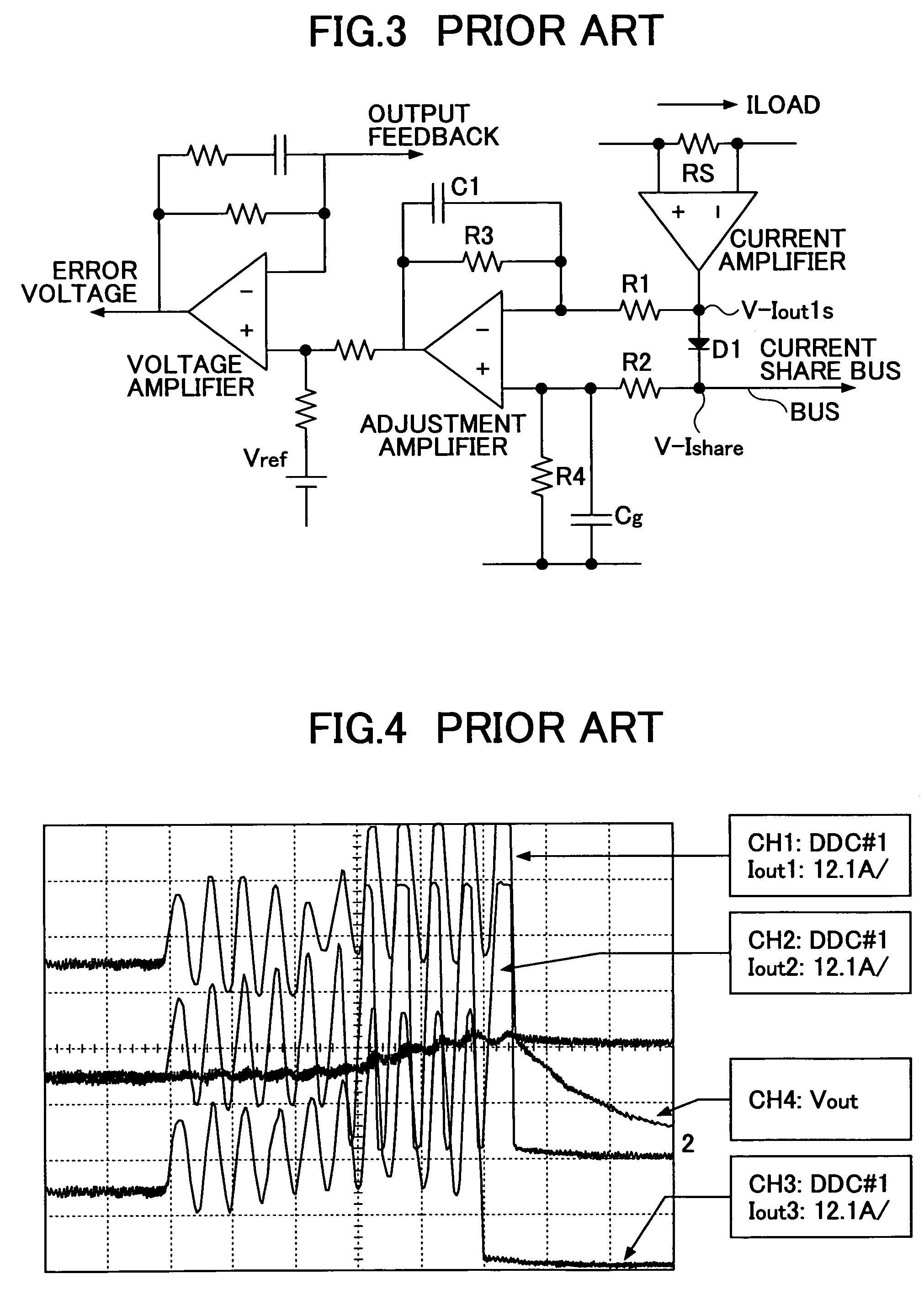
However, from about the fifth cycle, the output currents of the DDCs start to differ in size from and be out of phase with one another, and the output voltage starts to rise from 2.5 V, and finally, rises up to 3.3 V. As a result, an overvoltage protection circuit functions to stop the operation of each DDC, thus causing system down.
Accordingly, it is difficult to discover its possibility with a test apparatus, and it is predicted that this phenomenon occurs in a field so as to result in a serious problem.
However, in the case of reducing the value of the resistor Rd, the following two problems occur.
However, in the case of POL, connection line inductance is low, and the load capacitor is small.
In this case, reducing the value of the resistor Rd to 10 kΩ cannot completely solve the problem of output voltage increase generated because of variations in the load current.

Method used


Image

  • Power supply
  • Power supply
  • Power supply

Examples


Embodiment Construction

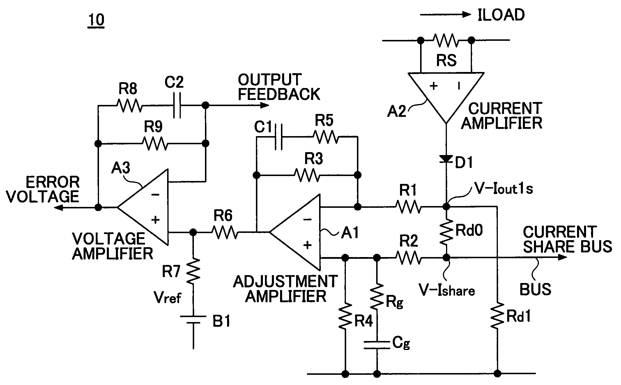
[0078]According to an embodiment of the present invention, in a power supply having parallel-connected multiple DDCs, a configuration shown in FIG. 10 is employed where a resistor Rd0 is connected between the current reference signal V-Ishare and the current detection signal V-Iout1s of a current balance circuit 10 of each DDC, and a resistor Rd1 is connected between the current detection signal V-Iout1s and ground (GND).

[0079]As a result, in the DDC, if V-Ishare is higher than an electric potential indicating its own output current (the output potential of a current detection amplifier A2), V-Iout1s increases through the resistor Rd0 in accordance with V-Ishare. As a result, the maximum value of the current detection signal V-Iout1s matches the current reference signal V-Ishare (FIGS. 15A and 15C). Thus, current balance control that follows up a maximum current value is enabled.

[0080]On the other hand, in the case of a conventional circuit configuration, the diode D1 is connected b...


PUM


Abstract

A power supply to be connected in parallel to one or more other power supplies so as to share with the other power supplies in supplying load current to a load is disclosed. The power supply includes a load current comparison part including a first input terminal and a second input terminal and outputting a difference in level between a first signal applied to the first input terminal and a second signal applied to the second input terminal. The load current comparison part includes a differential amplifier. A first input terminal of the differential amplifier is connected to a first input terminal of the differential amplifier of each of the other power supplies. A signal indicating a load current supplied by the power supply is input to a second input terminal of the differential amplifier. A non-directional impedance element is inserted between the first and second input terminals of the differential amplifier.

Description

BACKGROUND OF THE INVENTION[0001]1. Field of the Invention[0002]The present invention relates generally to power supplies, and more particularly to a power supply configured to be connected in parallel to one or more power supplies so as to share with the other power supplies in supplying load current.[0003]2. Description of the Related Art[0004]In recent years, so-called POL (Point of Load), which puts small-capacity DC / DC converters (hereinafter simply referred to as DDCs) into parallel operation and places them in the immediate vicinity of a load, has been commonly employed instead of the conventional centralized power architecture as power supply configuration for large-scale server systems. At this point, in order to increase the reliability of the DDCs operating in parallel, a so-called current balance function that equalizes the output currents of the DDCs for thermal balance among the DDCs is provided. As this current balance function, the average current mode, in which a DD...

Claims


Application Information

Patent Timeline
Patent Type & Authority Patents(United States)
IPC IPC(8): H02J1/10
CPCH02J1/102H02M3/155
Inventor ITAKURA, KAZUHIKOSHIMAMORI, HIROSHIAOKI, ISAMU
Owner FDK CORP
Learn More