Group III nitride semiconductor light emitting device

a technology of nitride semiconductor and light-emitting device, which is applied in the direction of solid-state devices, lasers, semiconductor lasers, etc., can solve the problems of inconvenient led installation, and achieve the effects of reducing the edge barrier of the conduction band, reducing the number of electrons, and increasing the fixed charge monotonously

Inactive Publication Date: 2007-05-17
PANASONIC CORP
View PDF1 Cites 243 Cited by
  • Summary
  • Abstract
  • Description
  • Claims
  • Application Information

AI Technical Summary

Benefits of technology

[0011]FIG. 12 is a graph showing calculation results for the relationship between a difference Δa0 between a lattice constant of the undoped second intermediate layer 107b in an a-axis direction in a lattice relaxed state and a lattice constant of the p-type electron blocking layer 108 in the a-axis direction in a lattice relaxed state and a fixed charge σ induced by the piezo effect on an interface between the undoped second intermediate layer 107b and p-type electron blocking layer 108. In this case, the fixed charge σ and the difference Δa0 are values obtained in the case wh...

Problems solved by technology

Note that such inconvenience might occur in a L...

Method used


Image

  • Group III nitride semiconductor light emitting device
  • Group III nitride semiconductor light emitting device
  • Group III nitride semiconductor light emitting device

Examples


embodiments

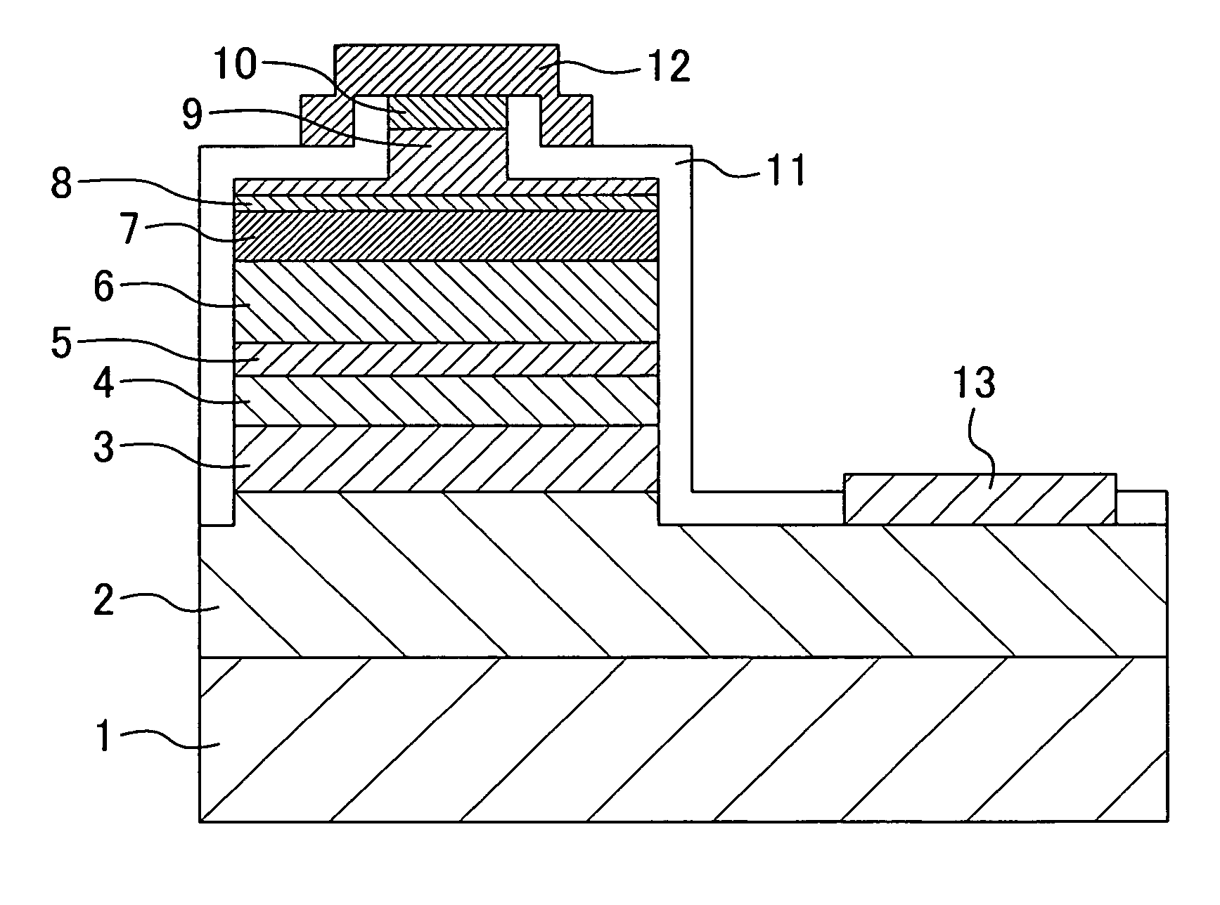
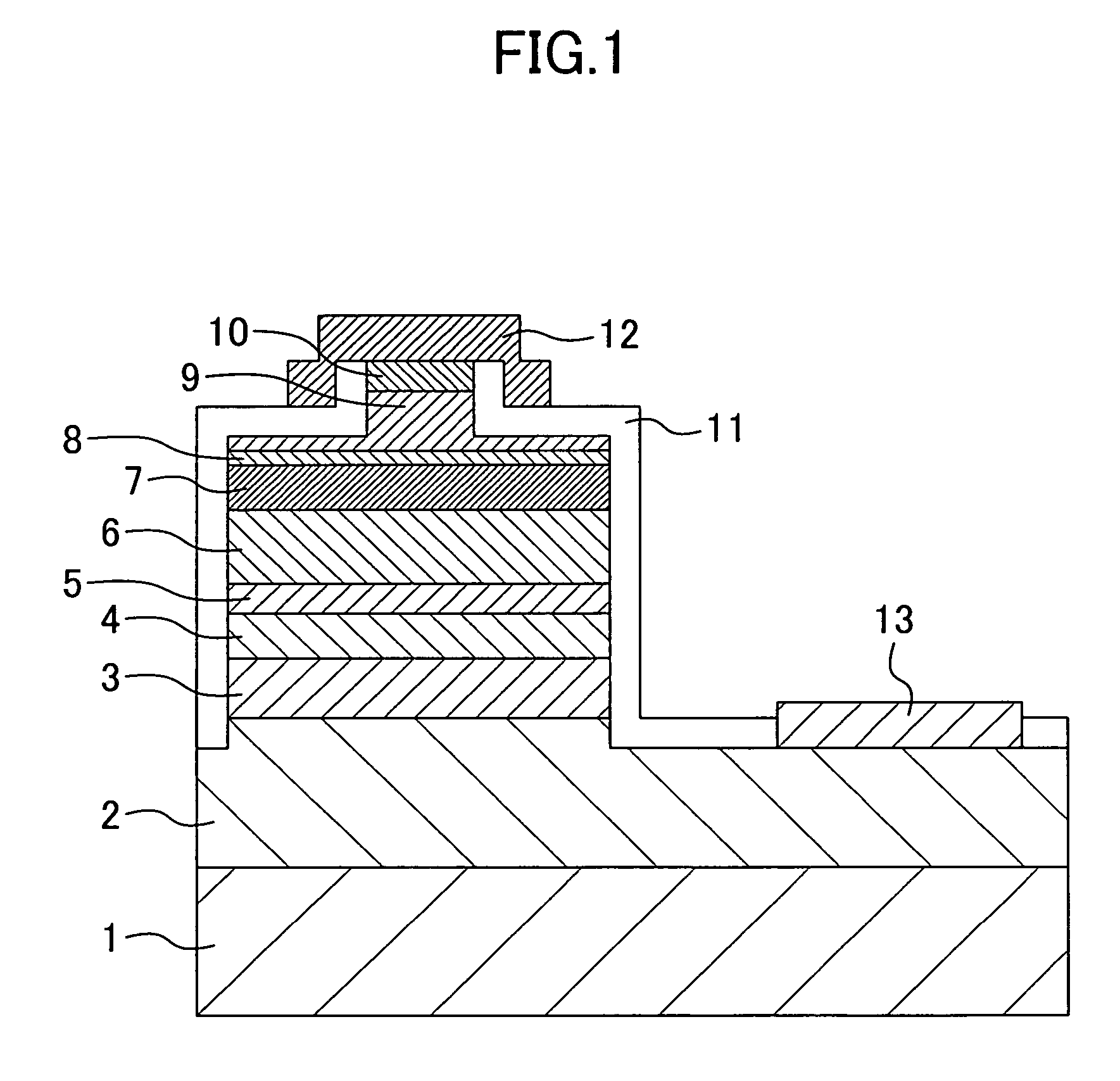
[0035] A semiconductor light emitting device according to an embodiment of the present invention will be described with reference to FIG. 1.

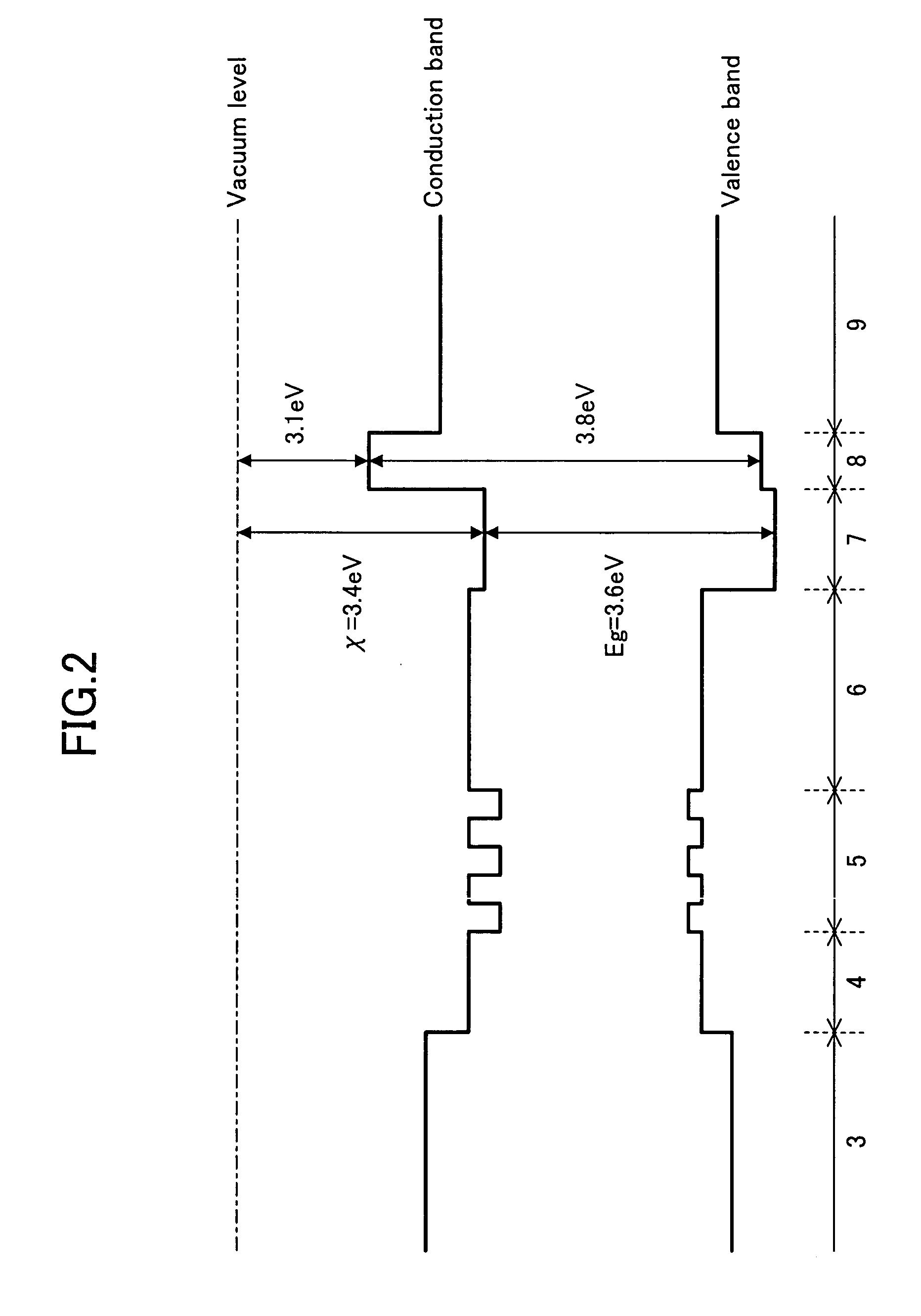
[0036]FIG. 1 is a cross-sectional view illustrating a structure of a semiconductor laser diode according to an embodiment of the present invention. FIG. 2 is a band diagram of the semiconductor laser diode of this embodiment.

[0037] As shown in FIG. 1, the semiconductor laser diode of this embodiment includes, a substrate 1, for example, made of sapphire, a low temperature buffer layer (not shown) made of GaN, an n-type contact layer 2 made of n-type group III nitride semiconductor, an n-type cladding layer 3 made of n-type group III nitride semiconductor, an n-side light guide layer 4 made of n-type group III nitride semiconductor, a multi-quantum well (MQW) active layer 5 made of undoped group III nitride semiconductor and having a smaller bandgap energy than that of the n-type cladding layer 3, a p-side light guide layer 6 made of undoped gr...


PUM


Abstract

A group III nitride semiconductor light emitting device according to the present invention includes an immediate layer formed of AlxGa1-x-yInyN (0<x<1, 0<y<1, x+y<1) between an active layer and a cladding layer and an electron blocking layer formed of p-type group III nitride semiconductor having a smaller electron affinity than that of the intermediate layer so as to be in contact with the intermediate layer. The semiconductor light emitting layer may be a laser diode or a LED.

Description

BACKGROUND OF THE INVENTION [0001] 1. Field of the Invention [0002] The present invention relates to a semiconductor light emitting device using group III nitride semiconductor. [0003] 2. Description of the Related Art [0004] In recent years, there have been increased demands for semiconductor laser diodes capable of outputting blue violet light as a light source for next generation high-density optical disks. Thus, an increased number of research and development of group III nitride semiconductor, i.e., direct energy-gap semiconductor having a forbidden band of 1.9 eV to 6.2 eV have been carried out. [0005] Among light emitting devices including group III nitride semiconductor, to increase confinement of light and suppress dispersion of magnesium (Mg) from a p-type cladding layer to an active layer, a laser diode is formed to have a structure in which an optical guide layer and an intermediate layer are formed between the active layer and the p-type cladding layer. Furthermore, the...

Claims


Application Information

Patent Timeline
IPC IPC(8): H01S5/00H01S3/04H01S5/22
CPCH01S5/32341
Inventor SUGIURA, KATSUMI
Owner PANASONIC CORP
Why Eureka
Try Eureka