Movable radiant heat sources

a technology of radiant heat source and moving element, which is applied in the field of heating systems, can solve the problems of inability failure to meet the requirements of the application,

Active Publication Date: 2010-05-25
ASM IP HLDG BV
View PDF12 Cites 247 Cited by
  • Summary
  • Abstract
  • Description
  • Claims
  • Application Information

AI Technical Summary

Problems solved by technology

If a CVD process step produces deposited layers with non-uniformities, devices at different areas on the wafer and even devices within the chips may have inconsistent operation characteristics, or may fail altogether.
If the temperature varies across the surface of the substrate, uneven deposition of the reactant gas occurs and the thickness and resistivity will not be uniform.
Radiant energy has a tendency to create non-uniform temperature distributions, including areas of less intensity (or shadows or “cold spots”) and areas of more intensity (or “hot spots”) due to the use of localized lamps and the consequent focusing and interference effects.
However, radiant heat sources still tend to induce hot and cold spots on wafers being heated.
However, it has been found that temperature uniformity suffers even with this continual rotation of the wafer or the reflector bank about a vertical axis.

Method used


Image

  • Movable radiant heat sources
  • Movable radiant heat sources
  • Movable radiant heat sources

Examples


Embodiment Construction

[0023]Although certain preferred embodiments and examples are disclosed below, it will be understood by those in the art that the invention extends beyond the specifically disclosed embodiments and / or uses of the invention and obvious modifications and equivalents thereof. Thus, it is intended that the scope of the invention herein disclosed should not be limited by the particular disclosed embodiments described below.

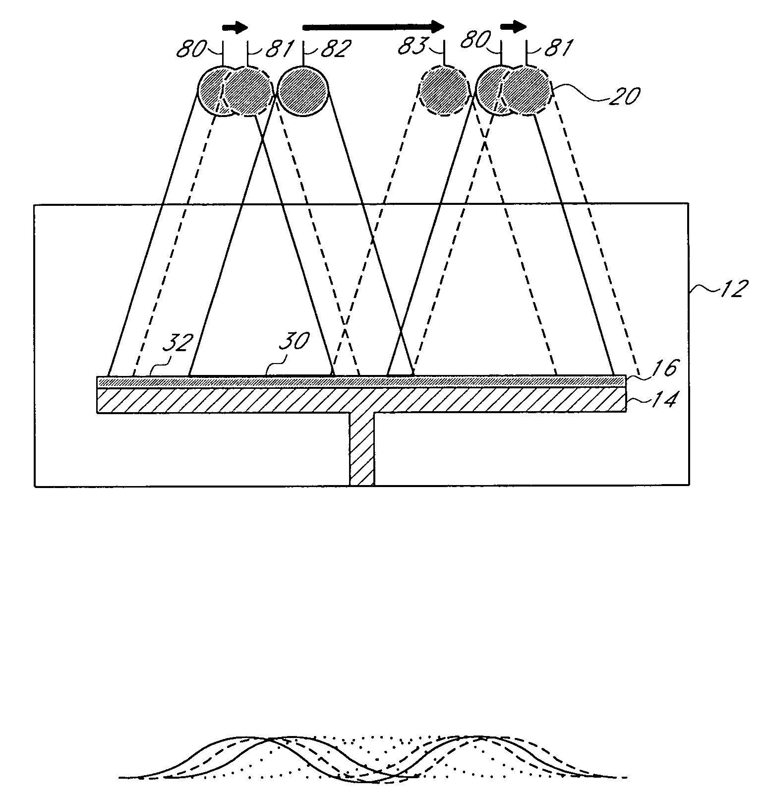
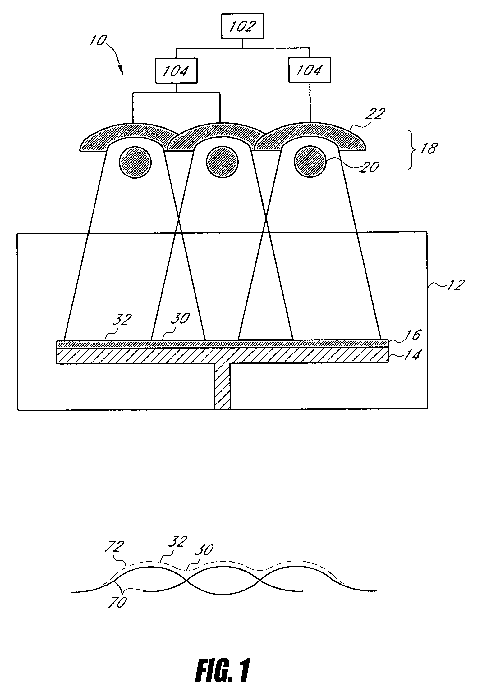
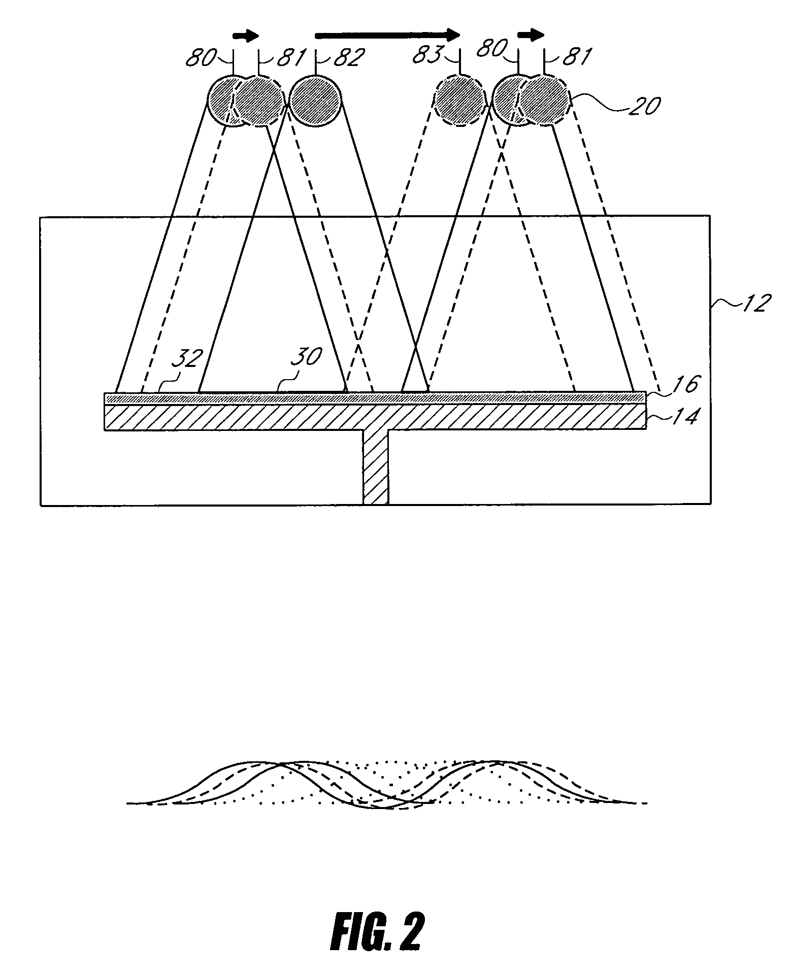
[0024]FIG. 1 is a schematic side view of one example of a semiconductor processing apparatus 10 with a movable radiation device. The apparatus 10 comprises a process chamber 12, a support structure 14 within the chamber 12 configured for supporting a workpiece 16, and a plurality of radiant heat sources. The radiant heat sources may comprise bulbs 20, reflectors 22, or a lamp 18, which is a combination of a bulb 20 and a reflector 22. A plurality of heat sources may be referred to as an array or a bank (e.g., a lamp bank comprises a plurality of lamps 18). The radiant ...


PUM

PropertyMeasurementUnit
angleaaaaaaaaaa
angleaaaaaaaaaa
angleaaaaaaaaaa

Abstract

A semiconductor processing apparatus including a processing chamber and a plurality of radiant heat sources. The radiant heat sources heat a workpiece within the chamber. At least one of the radiant heat sources is movable during processing in an oscillatory motion along a path less than about 10 mm from a geometric center of the oscillatory motion.

Description

BACKGROUND OF THE INVENTION[0001]1. Field of the Invention[0002]The invention generally relates to heating systems for semiconductor manufacturing equipment. More specifically, the invention relates to radiant heat sources for improving temperature uniformity.[0003]2. Description of the Related Art[0004]Chemical vapor deposition (CVD) is a very well known process in the semiconductor industry for forming thin films of materials on wafers. In a CVD process, gaseous molecules of the material to be deposited are supplied to wafers to form a thin film of that material on the wafers by chemical reaction. Such formed thin films may be polycrystalline, amorphous, or epitaxial. Typically, CVD processes are conducted at elevated temperatures in order to accelerate the chemical reaction.[0005]In the semiconductor industry, it is important that the material be deposited with uniform properties, such as thickness and composition, over the wafer. In Very Large and Ultra Large Scale Integrated Ci...

Claims


Application Information

Patent Timeline
Patent Type & Authority Patents(United States)
IPC IPC(8): A21B2/00C23C16/00
CPCH01L21/67115
Inventor AGGARWAL, RAVINDERSTOUTJESDIJK, JEROEN
Owner ASM IP HLDG BV
Why Eureka
Try Eureka