Nonvolatile phase change memory cell having a reduced contact area

a phase change memory, nonvolatile technology, applied in the direction of bulk negative resistance effect devices, electrical equipment, semiconductor devices, etc., can solve the problem of difficult to reduce the contact area below photolithographic limits

Inactive Publication Date: 2010-06-01
SANDISK CORP
View PDF34 Cites 83 Cited by
  • Summary
  • Abstract
  • Description
  • Claims
  • Application Information

AI Technical Summary

Problems solved by technology

It can be difficult to reduce this contact area below photolithographic limits, however.

Method used


Image

  • Nonvolatile phase change memory cell having a reduced contact area
  • Nonvolatile phase change memory cell having a reduced contact area
  • Nonvolatile phase change memory cell having a reduced contact area

Examples


example

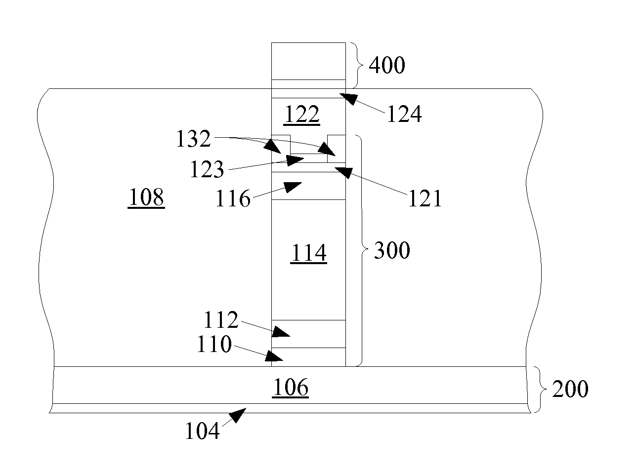
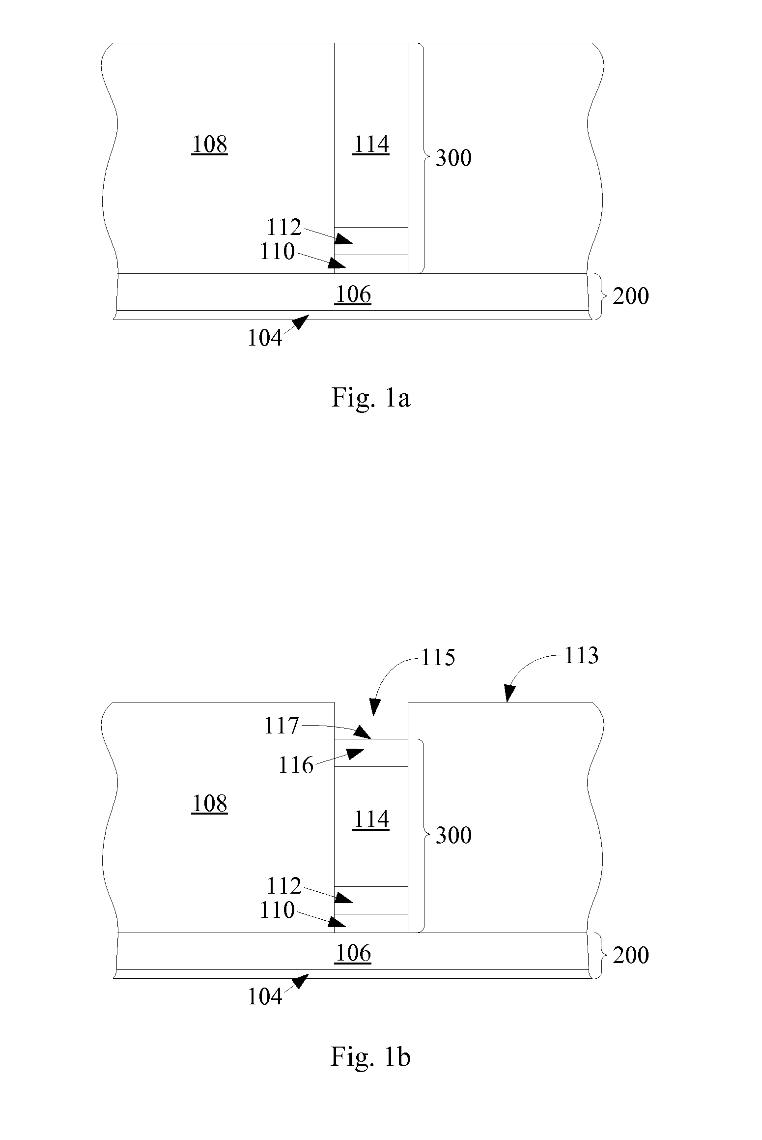
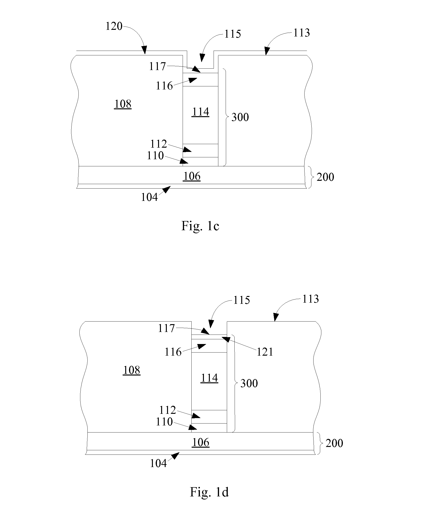
[0041]Fabrication of a single memory level formed above a substrate will be described in detail. Additional memory levels can be stacked, each monolithically formed above the one below it.

[0042]Turning to FIG. 4a, formation of the memory begins with a substrate 100. This substrate 100 can be any semiconducting substrate as known in the art, such as monocrystalline silicon, IV-IV compounds like silicon-germanium or silicon-germanium-carbon, III-V compounds, II-VII compounds, epitaxial layers over such substrates, or any other semiconducting material. The substrate may include integrated circuits fabricated therein.

[0043]An insulating layer 102 may be formed over the substrate 100. The insulating layer 102 can be silicon oxide, silicon nitride, high-dielectric film, Si—C—O—H film, or any other suitable insulating material.

[0044]First conductors 200 are formed over the substrate and insulator. An adhesion layer 104 may be included between insulating layer 102 and conducting layer 106 t...


PUM


Abstract

A nonvolatile memory cell having a contact area between a phase-change material such as a chalcogenide and a heat source which is smaller than photolithographic limits is described. To form this cell, a conductive or semiconductor pillar is exposed at a dielectric surface and recessed by selective etch. A thin, conformal layer of a spacer material is deposited on the dielectric top surface, the pillar top surface, and the sidewalls of the recess, then removed from horizontal surfaces by anistropic etch, leaving a spacer on the sidewalls defining a reduced volume within the recess. The phase change material is deposited within the spacer, having a reduced contact area to the underlying conductive or semiconductor pillar.

Description

RELATED APPLICATIONS[0001]This application is related to Raghuram et al., U.S. patent application Ser. No. 11 / 560,792, “Method of Making a Nonvolatile Phase Change Memory Cell Having a Reduced Contact Area,” filed on even date herewith and hereby incorporated by reference.BACKGROUND OF THE INVENTION[0002]The invention relates to a nonvolatile memory cell including a phase-change element, such as an element formed of a chalcogenide. Heat is required to convert a phase-change element between phases, and heat provided to the phase-change element can be focused by decreasing the contact area between the phase-change element and the heat source. It can be difficult to reduce this contact area below photolithographic limits, however.[0003]There is a need, therefore, for a method to form a contact area that is smaller the minimum feature size that can be formed photolithographically.SUMMARY OF THE PREFERRED EMBODIMENTS[0004]The present invention is defined by the following claims, and noth...

Claims


Application Information

Patent Timeline
Patent Type & Authority Patents(United States)
IPC IPC(8): H01L29/02
CPCH01L27/2409H01L27/2481H01L45/06H01L45/1691H01L45/126H01L45/144H01L45/1683H01L45/1233H10B63/20H10B63/84H10N70/8413H10N70/231H10N70/826H10N70/8828H10N70/068H10N70/066
Inventor RAGHURAM, USHAHERNER, S. BRAD
Owner SANDISK CORP
Why Eureka
Try Eureka