Self-aligned manufacturing method, and manufacturing method for thin film fuse phase change ram

a manufacturing method and phase change technology, applied in the direction of electrical equipment, digital storage, instruments, etc., can solve the problems of inability to resolve objects, the need for smaller feature sizes, and the limitations of current fabrication processes in terms of the smallest devices possible using known techniques,

Active Publication Date: 2007-07-26
MACRONIX INT CO LTD
View PDF98 Cites 196 Cited by
  • Summary
  • Abstract
  • Description
  • Claims
  • Application Information

AI Technical Summary

Problems solved by technology

As is well known, current fabrication processes are encountering limitations in terms of the smallest devices possible using known techniques.
The smallest feature that can be formed using a given process is referred to as the “minimum feature size.” As size requirements have become smaller, however, the need for smaller feature sizes has come up against problems such as the wavelength of light—one cannot resolve objects smaller than the wavelength of the light being used.
The art has recognized this problem but has not presented a solution that allows formation of features in the range of 100 nm and less.
No solutions below that level are offered, however.
Problems have arisen in manufacturing such devices with very small dimensions, and with variations in process that meets tight specifications needed for large-scale memory devices.

Method used


Image

  • Self-aligned manufacturing method, and manufacturing method for thin film fuse phase change ram
  • Self-aligned manufacturing method, and manufacturing method for thin film fuse phase change ram
  • Self-aligned manufacturing method, and manufacturing method for thin film fuse phase change ram

Examples


Embodiment Construction

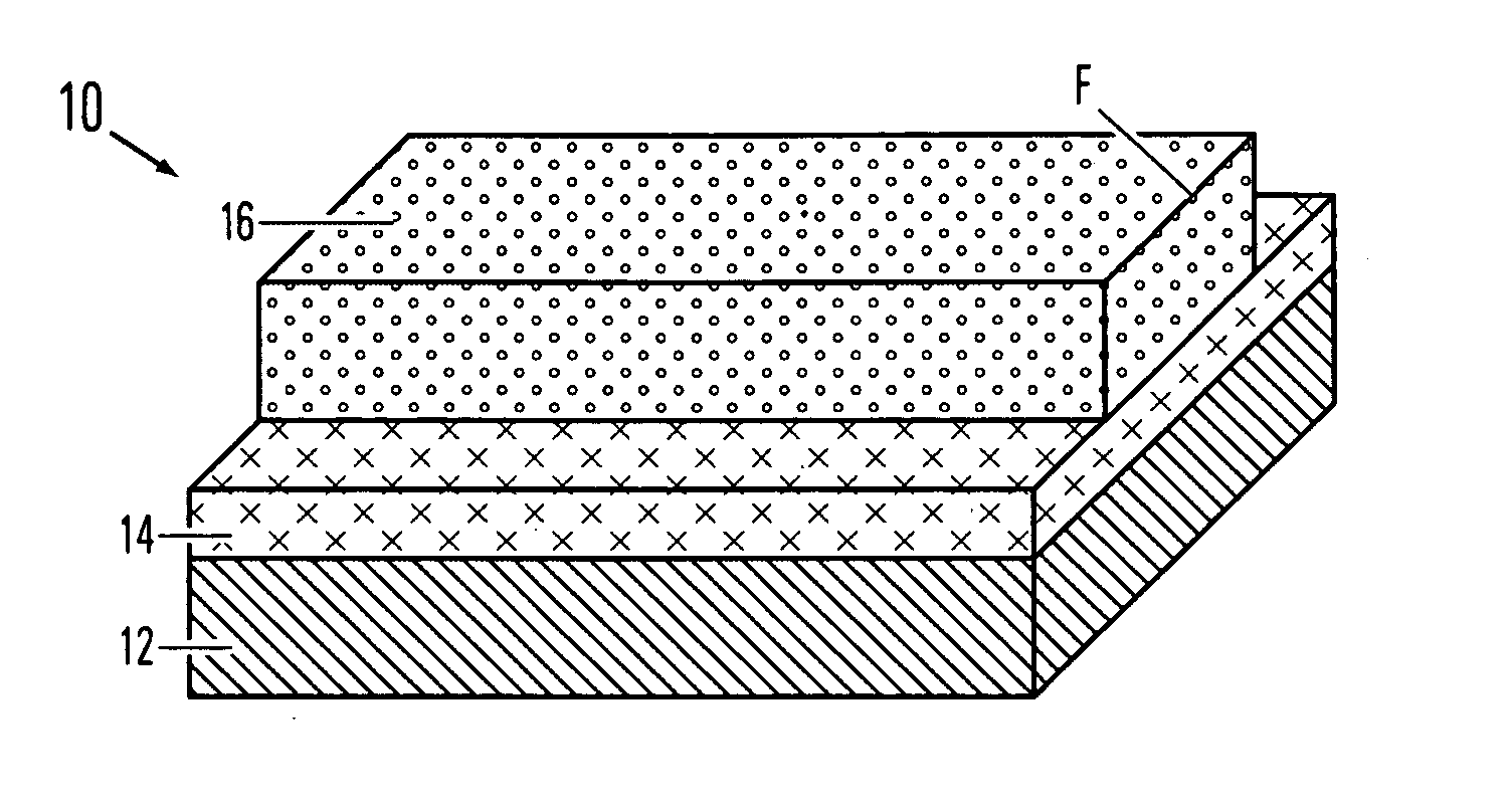
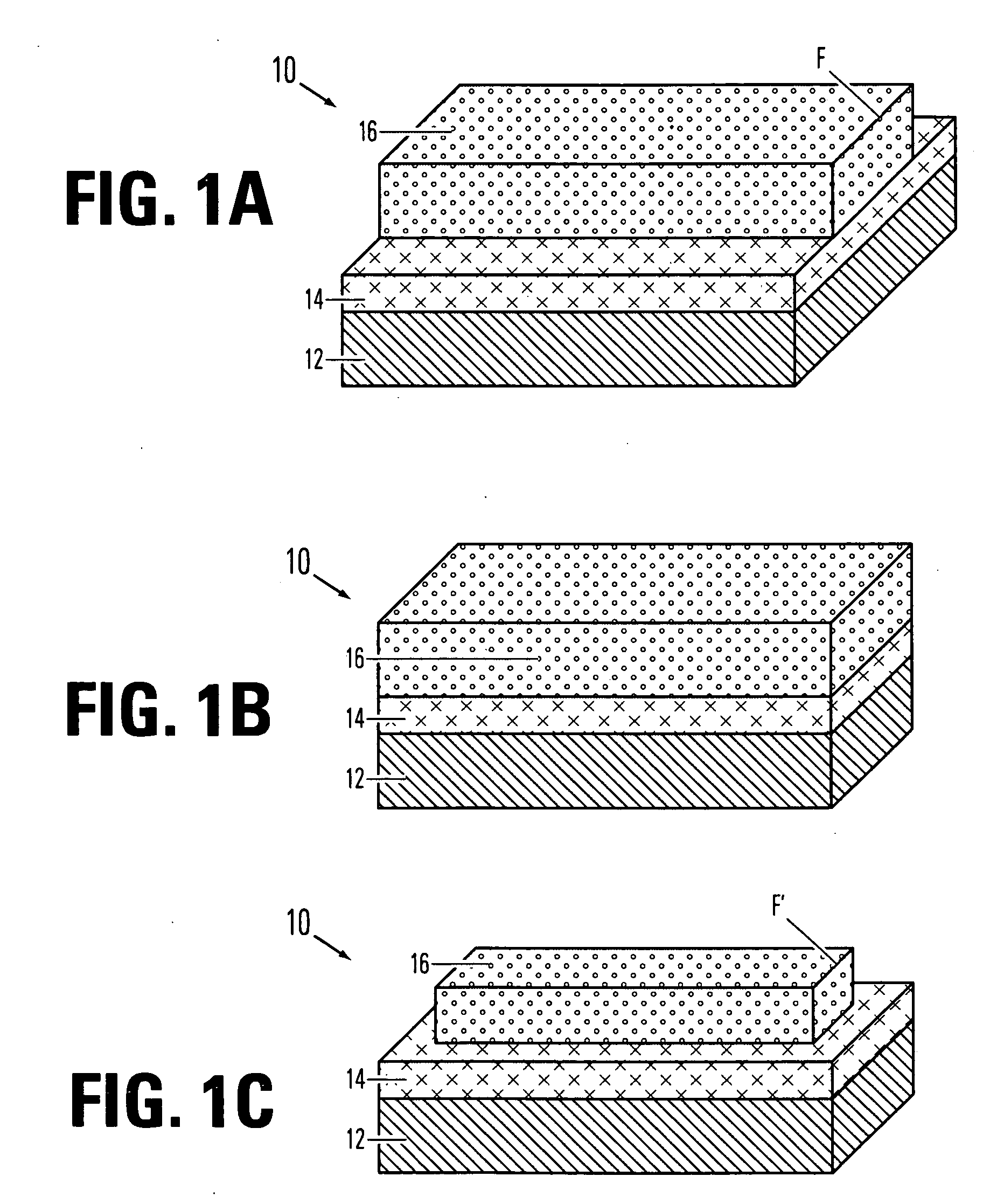
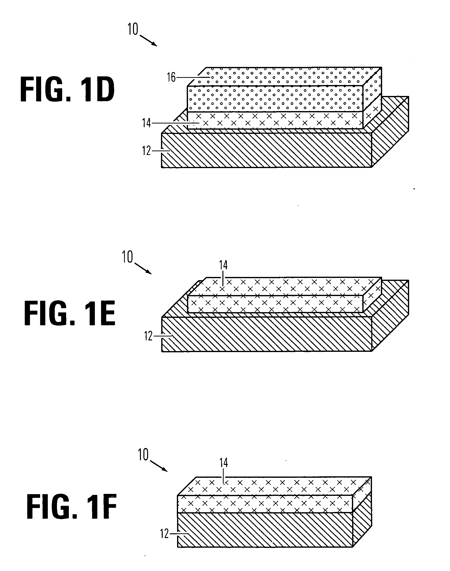
[0015] A detailed description of thin film fuse phase change memory cells, arrays of such memory cells, and methods for manufacturing such memory cells, is provided with reference to FIGS. 1-5.

[0016] A common sequence in semiconductor fabrication is to deposit a material, either in a single layer or multilayered structure, and then etch that material, either to reduce its lateral extent or to form openings or trenches in the material. In either event, the conventional process for accomplishing those tasks, generally referred to as lithography, involves depositing a layer of resist material, patterning the resist so that the areas to be cut are exposed, and etching the exposed areas to form the chip features desired. As previously noted, conventional technique would call for a different lithographic process for each iteration of patterning and etching. As also discussed above, however, a requirement to form features having dimensions smaller than the minimum feature size of a proces...


PUM


Abstract

A method for manufacturing a self aligned narrow structure over a wider structure based on mask trimming. A method for manufacturing a memory device comprises forming an electrode layer on a substrate which comprises circuitry made using front-end-of-line procedures. The electrode layer includes a first electrode and a second electrode, and an insulating member between the first and second electrodes for each phase change memory cell to be formed. A patch of memory material is formed on the top surface of the electrode layer across the insulating member for each memory cell to be formed. The patch and the first and second electrodes are formed using a self-aligned process based on mask trimming.

Description

PARTIES TO A JOINT RESEARCH AGREEMENT [0001] International Business Machines Corporation, a New York corporation; Macronix International Corporation, Ltd., a Taiwan corporation; and Infineon Technologies A.G., a German corporation, are parties to a Joint Research Agreement. BACKGROUND OF THE INVENTION [0002] 1. Field of the Invention [0003] The present invention relates to fabrication of semiconductor devices, and most specifically to the fabrication of semiconductor devices at sub-lithographic sizes. [0004] 2. Description of Related Art [0005] The operation of Moore's Law, which holds that the number of transistors on an integrated circuit will double every 18 months, clearly requires ever smaller devices. As is well known, current fabrication processes are encountering limitations in terms of the smallest devices possible using known techniques. Conventional processes are built around deposition and etching, employing photoresistive etch masks. Generally, layers of materials are d...

Claims


Application Information

Patent Timeline
Patent Type & Authority Applications(United States)
IPC IPC(8): H01L21/302H01L21/461
CPCG11C13/0004H01L21/0338H01L45/1226H01L45/148H01L45/1675H01L45/144H01L45/06H01L45/1233H01L45/126H01L45/143H01L45/1691H10N70/823H10N70/231H10N70/8413H10N70/8825H10N70/884H10N70/826H10N70/8828H10N70/068H10N70/063
Inventor LUNG, HSIANG-LAN
Owner MACRONIX INT CO LTD
Why Eureka
Try Eureka