Electrically programmable memory element with improved contacts

a memory element and contact technology, applied in the direction of digital storage, semiconductor/solid-state device details, instruments, etc., can solve the problems of inconsequential or at best unsubstantial power saving, relative high energy input required to obtain detectable changes, etc., to reduce cell area and reduce programming energy

Inactive Publication Date: 2005-11-29
OVONYX MEMORY TECH LLC
View PDF9 Cites 201 Cited by
  • Summary
  • Abstract
  • Description
  • Claims
  • Application Information

AI Technical Summary

Benefits of technology

[0013]An object of the present invention is to provide a memory element having reduced programmin...

Problems solved by technology

The most significant of these limitations was the relatively high energy input required to obtain detectable changes in the chemical and/or electronic bonding configurations of the chalcogenide material in order to initiate a detectable change in local order.
Such high energy levels translate into high current carrying re...

Method used


Image

  • Electrically programmable memory element with improved contacts
  • Electrically programmable memory element with improved contacts
  • Electrically programmable memory element with improved contacts

Examples


Embodiment Construction

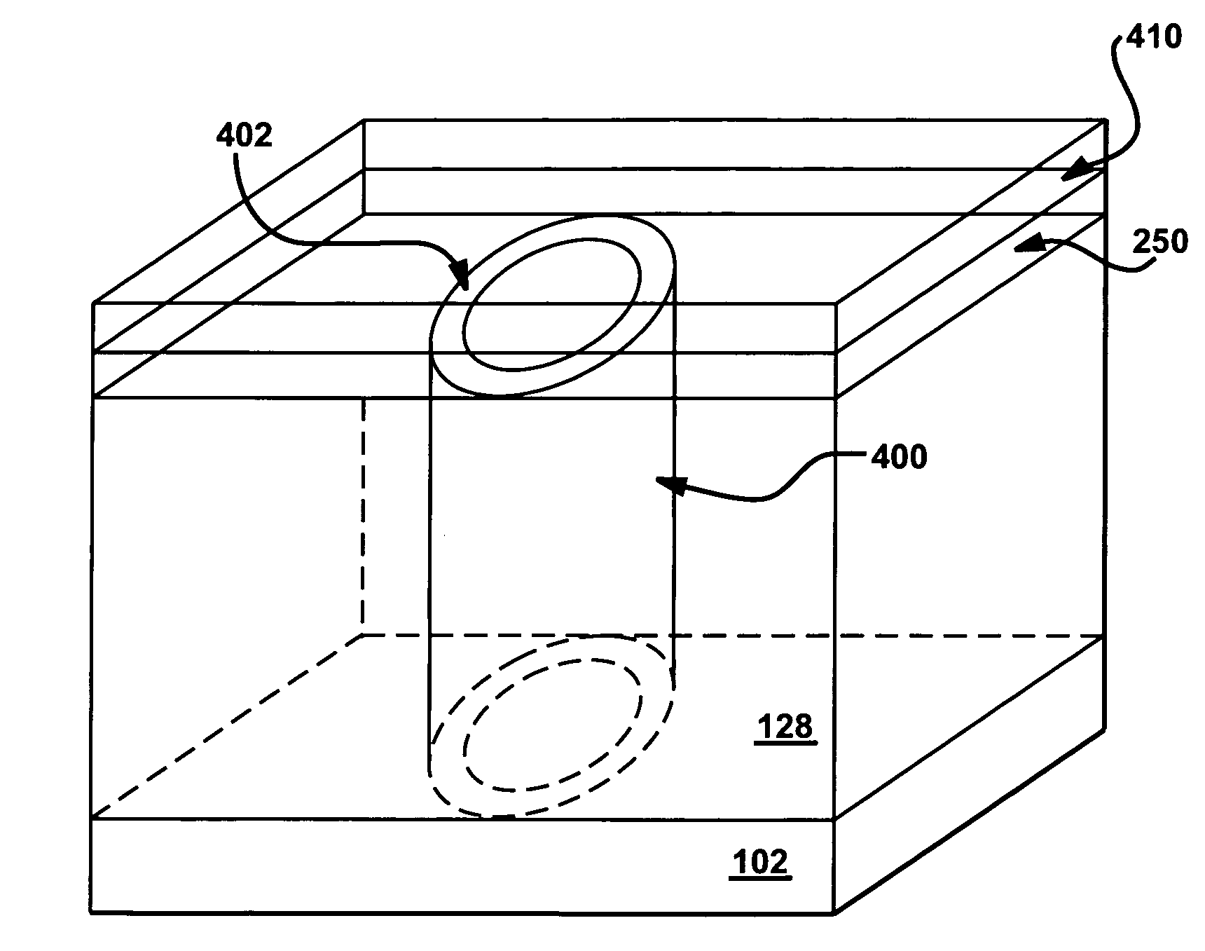
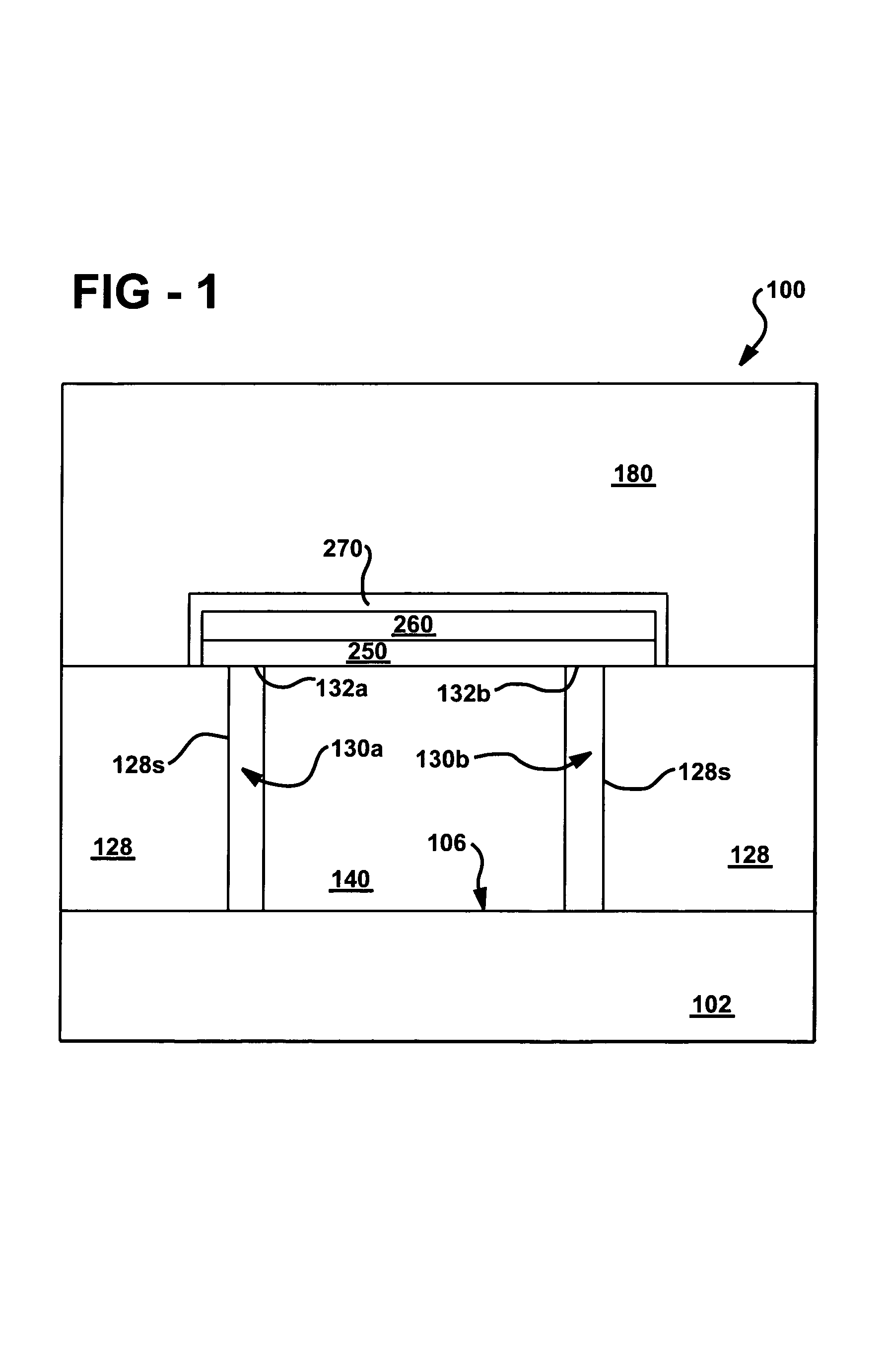
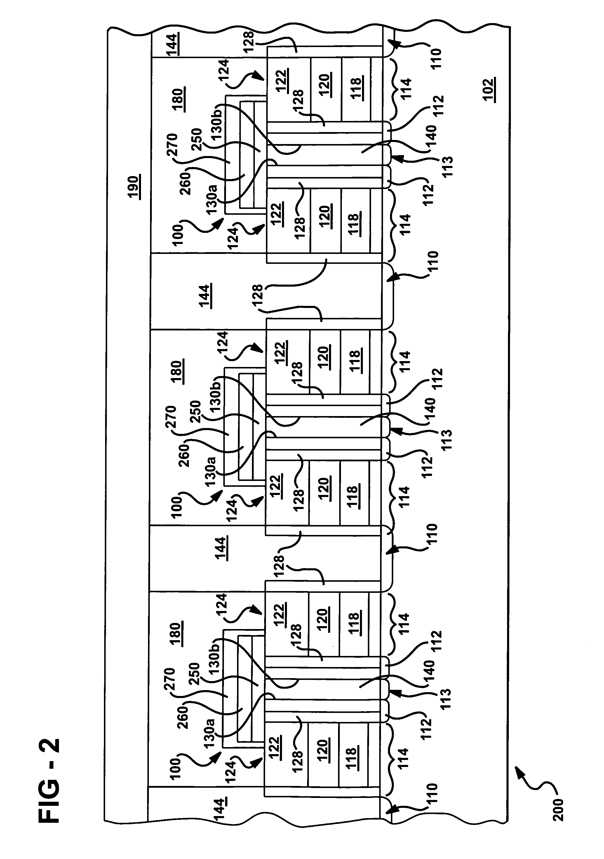
[0033]FIG. 1 is a cross-sectional view of a memory device 100 of the present invention formed on a semiconductor substrate 102. The memory device 100 comprises two independent single-cell memory elements. The first single-cell memory element comprises a first contact 130A, memory material layer 250, and second contact 270. The second single-cell memory element comprises first contact 130B, memory material layer 250, and second contact 270. As shown in the embodiment shown in FIG. 1, two memory elements may share a single continous volume of phase change memory material. The insulative layer 260 provides for electrical isolation between the memory material 250 and the horizontally disposed section of the second contact 270. The insulative layer 260 also provides a thermal blanket keeping heat energy within the memory material layer 250. The dielectric region 140 electrically isolates the first contact 130A from the first contact 130B. The first contacts 130A,B and the second contact ...


PUM


Abstract

A memory element comprising a volume of phase change memory material; and first and second contact for supplying an electrical signal to the memory material, wherein the first contact comprises a conductive sidewall spacer. Alternately, the first contact may comprise a contact layer having an edge adjacent to the memory material.

Description

RELATED APPLICATION INFORMATION[0001]This application is a continuation-in-part of U.S. patent application Ser. No. 08 / 942,000, filed Oct. 1, 1997 now abandoned.FIELD OF THE INVENTION[0002]The present invention relates generally to a uniquely designed solid state, electrically operated memory element. More specifically, the present invention relates to a new structural relationship between the electrical contacts and the memory material which are integral parts of the memory element.BACKGROUND AND PRIOR ART[0003]The Ovonic EEPROM is a proprietary, high performance, non-volatile, thin-film electronic memory device. Its advantages include non-volatile storage of data, potential for high bit density and, consequently, low cost because of its small footprint and simple two-terminal device configuration, long reprogramming cycle life, low programming energies and high speed. The Ovonic EEPROM is capable of both analog and digital forms of information storage. Digital storage can be eithe...

Claims


Application Information

Patent Timeline
IPC IPC(8): G11C11/56H01L27/24H01L45/00
CPCG11C11/56G11C11/5678H01L45/06H01L45/1233H01L45/122H01L45/144H01L45/16H01L45/1675H01L27/2436H01L27/2472H01L45/126G11C13/0004H10B63/30H10B63/82H10N70/231H10N70/821H10N70/826H10N70/8413H10N70/8828H10N70/011H10N70/063
Inventor LOWREY, TYLEROVSHINSKY, STANFORD R.WICKER, GUY C.KLERSY, PATRICK J.PASHMAKOV, BOILCZUBATYJ, WOLODYMYRKOSTYLEV, SERGEY A.
Owner OVONYX MEMORY TECH LLC
Why Eureka
Try Eureka