Silicon carbide UMOSFET device integrated with SBD

A technology of silicon carbide and devices, which is applied in the direction of semiconductor devices, semiconductor/solid-state device manufacturing, electrical components, etc., can solve the problems of weak internal freewheeling ability of silicon carbide UMOSFET devices, incapable device freewheeling, and increased system area, etc., to achieve Improve the anti-avalanche ability, improve the reliability of gate oxide, and reduce the effect of cell area

Inactive Publication Date: 2020-10-09
XIDIAN UNIV
View PDF6 Cites 0 Cited by
  • Summary
  • Abstract
  • Description
  • Claims
  • Application Information

AI Technical Summary

Problems solved by technology

However, due to the large bandgap of silicon carbide materials, the turn-on voltage of the parasitic PiN diodes integrated in silicon carbide UMOSFET devices is mostly around 3V, which cannot provide freewheeling for the device itself, resulting in the internal freewheeling capability of silicon carbide UMOSFET devices. weaker
Therefore, in power electronic system applications such as full bridges, an additional Schottky diode is often used in antiparallel as a freewheeling diode, which greatly increases the area of ​​the system
In addition, in the blocking mode, a series of reliability problems will be caused due to the strong electric field of the gate oxide at the corner of the trench

Method used


Image

  • Silicon carbide UMOSFET device integrated with SBD
  • Silicon carbide UMOSFET device integrated with SBD
  • Silicon carbide UMOSFET device integrated with SBD

Examples


Embodiment 1

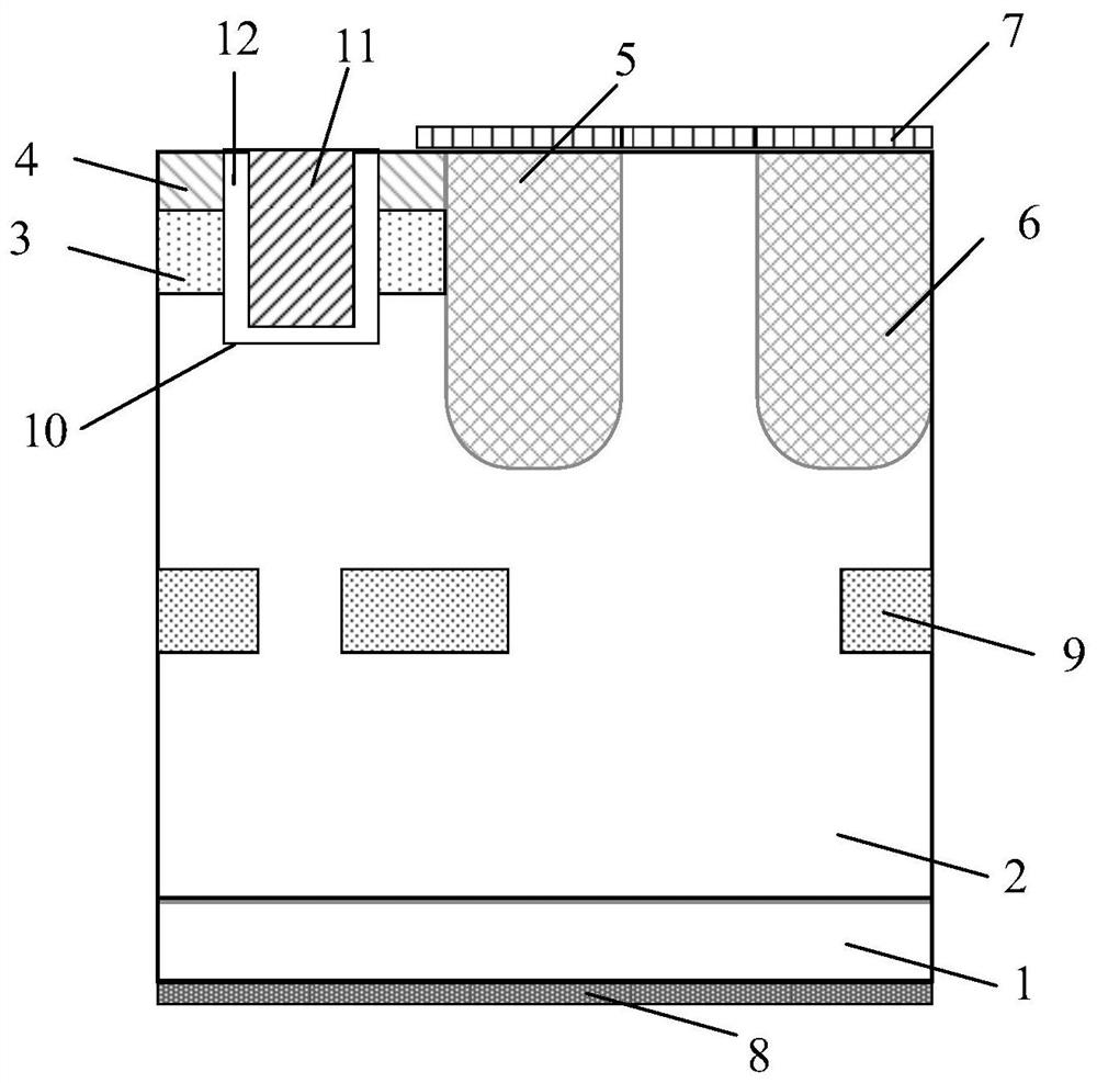
[0035] See figure 1 , figure 1 It is a schematic structural diagram of a silicon carbide UMOSFET device integrating SBD (Schottky Barrier Diode, Schottky diode) provided by an embodiment of the present invention. As shown in the figure, the silicon carbide UMOSFET device integrating SBD according to the embodiment of the present invention includes:

[0036] N+ substrate region 1;

[0037] The N- epitaxial region 2 is arranged on the N+ substrate region 1;

[0038] The P-well region 3 is located inside the N-epitaxial region 2;

[0039] The N+ implantation region 4 is arranged on the P-well region 3 and located inside the N-epitaxy region 2;

[0040] The gate is arranged inside the N-epitaxy region 2, the P-well region 3 and the N+ injection region 4;

[0041] The first P+ implantation region 5 is located inside the N- epitaxial region 2, and is adjacent to the P-well region 3 and the N+ implantation region 4, and the depth of the first P+ implantation region 5 is greater ...

Embodiment 2

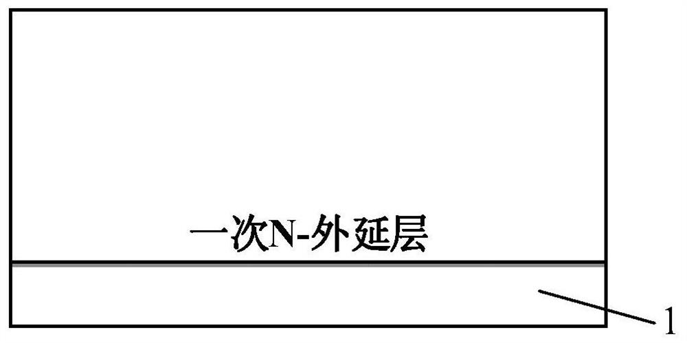
[0060] See Figure 2a-Figure 2i , Figure 2a-Figure 2i It is a process schematic diagram of an integrated SBD silicon carbide UMOSFET device provided by an embodiment of the present invention, and the preparation method includes the following steps:

[0061] Step a: Form an N- epitaxial layer on the N+ substrate region 1 by means of epitaxial growth, such as Figure 2a shown.

[0062] First, the thickness is 350 μm, and the doping concentration is 5×10 18 cm -3 The SiC substrate was cleaned by RCA standard, and then epitaxially grown on the N+ substrate region 1 with a thickness of 4 μm and a doping concentration of 6×10 15 cm -3 of the primary N-epitaxial layer.

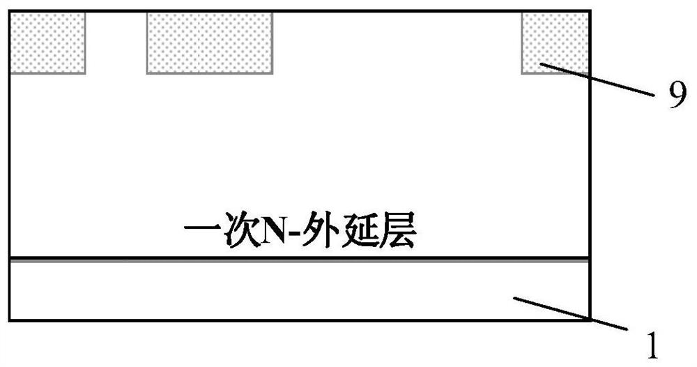
[0063] Step b: Perform ion implantation on the surface of the primary N- epitaxial layer to form several P+ ion implantation regions 9, such as Figure 2b shown.

[0064] With aluminum as a mask, selective Al ion implantation is performed on the primary N- epitaxial layer. The depth of each implanted region ...


PUM

PropertyMeasurementUnit
depthaaaaaaaaaa
widthaaaaaaaaaa
thicknessaaaaaaaaaa

Abstract

The invention relates to a silicon carbide UMOSFET device integrated with an SBD. The device comprises an N+ substrate region, an N- epitaxial region, a P-well region, an N+ injection region, a grid electrode, a first P+ injection region, a second P+ injection region, a source electrode and a drain electrode, wherein the depths of the first P+ injection region and the second P+ injection region are greater than the depth of the grid electrode, the interface of the source electrode and the N+ injection region, the interface of the first P+ injection region and the interface of the second P+ injection region are in ohmic contact, and the interface of the source electrode and the N- epitaxial region are in Schottky contact. The Schottky diode structure is integrated in the device, so that anextra Schottky diode is prevented from being inversely connected in parallel to serve as a freewheeling diode in the application process, the freewheeling capability of the device is improved, meanwhile, the cellular area of the device is reduced, and the preparation cost of the device is reduced.

Description

technical field [0001] The invention belongs to the technical field of semiconductors, and in particular relates to a silicon carbide UMOSFET device integrating SBDs. Background technique [0002] In recent years, with the continuous development of power electronic systems, higher requirements have been placed on the power devices in the system. Silicon (Si)-based power electronic devices have been unable to meet the requirements of system applications due to the limitations of the material itself. As a representative of the third-generation semiconductor material, silicon carbide (SiC) materials are far better than silicon materials in many characteristics. Silicon carbide MOSFET (Metal-Oxide-Semiconductor Field-Effect Transistor, Metal-Oxide-Semiconductor Field-Effect Transistor) device, as a commercialized device in recent years, has an alternative in terms of on-resistance, switching time, switching loss and heat dissipation performance. The huge potential of the existi...

Claims


Application Information

Patent Timeline
Patent Type & Authority Applications(China)
IPC IPC(8): H01L29/78H01L21/336H01L29/06H01L29/16H01L29/423
CPCH01L29/0603H01L29/0684H01L29/1608H01L29/4236H01L29/66068H01L29/7827H01L29/7839H01L29/0623H01L29/7806H01L29/7813
Inventor 袁昊何艳静韩超汤晓燕宋庆文张玉明
Owner XIDIAN UNIV
Why Eureka
Try Eureka