Silicon carbide UMOSFET device integrated with TJBS

A silicon carbide and device technology, used in semiconductor devices, semiconductor/solid-state device manufacturing, electrical components, etc., can solve the problem of weak internal freewheeling capability of silicon carbide UMOSFET devices, increasing the complexity and cost of circuit systems, and incapable of device freewheeling. and other problems, to achieve the effect of improving the avalanche resistance, improving the breakdown characteristics, and improving the performance of the device

Active Publication Date: 2020-10-09
芜湖西晶微电子科技有限公司
View PDF4 Cites 0 Cited by
  • Summary
  • Abstract
  • Description
  • Claims
  • Application Information

AI Technical Summary

Problems solved by technology

However, due to the large bandgap of silicon carbide materials, the turn-on voltage of the parasitic PiN diodes integrated in silicon carbide UMOSFET devices is mostly around 3V, which cannot provide freewheeling for the device itself, resulting in the internal freewheeling capability of silicon carbide UMOSFET devices. weaker
Therefore, in power electroni

Method used


Image

  • Silicon carbide UMOSFET device integrated with TJBS
  • Silicon carbide UMOSFET device integrated with TJBS
  • Silicon carbide UMOSFET device integrated with TJBS

Examples


Example Embodiment

[0035] Example one

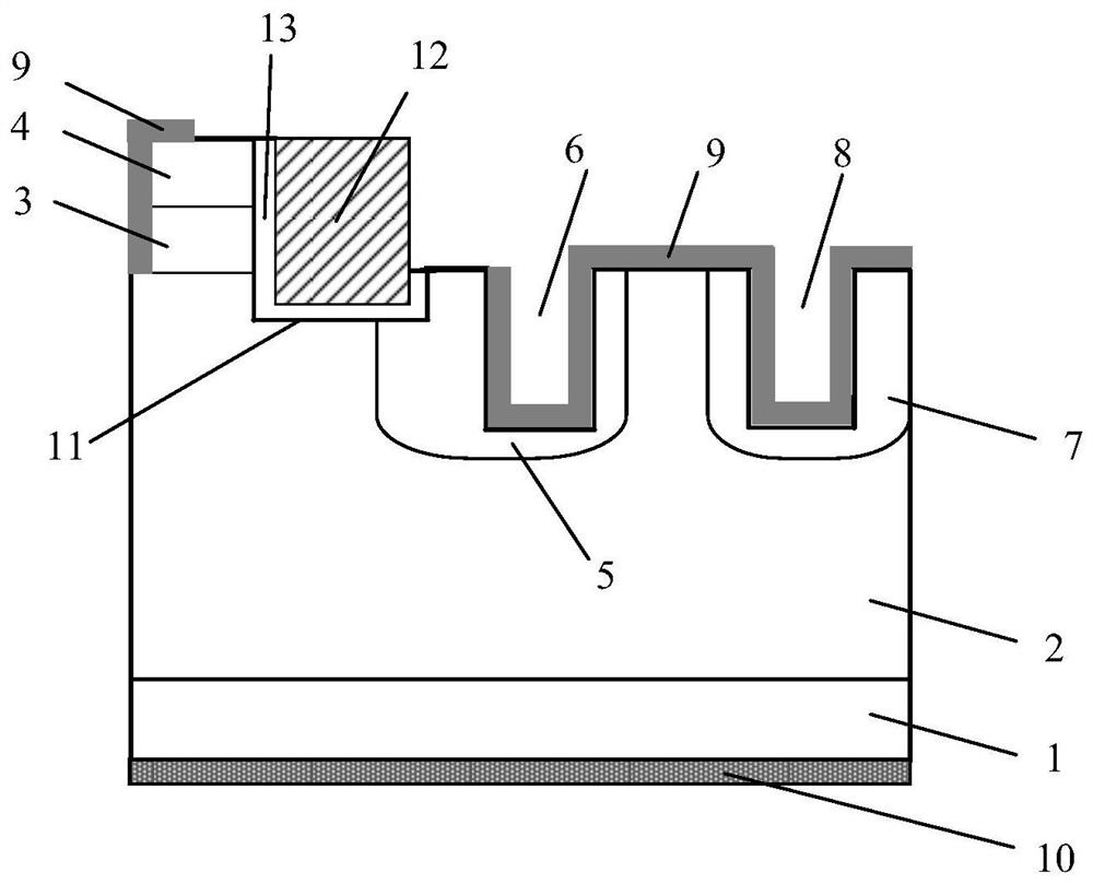
[0036] See figure 1 , figure 1 It is a schematic structural diagram of a silicon carbide UMOSFET device integrated with TJBS (Trenched Junction Barrier schottky) provided by an embodiment of the present invention. As shown in the figure, the integrated TJBS silicon carbide UMOSFET device of this embodiment includes:

[0037] N+ substrate area 1;

[0038] The N- epitaxial region 2 is arranged on the N+ substrate region 1;

[0039] The P-well region 3 is arranged on the N-epitaxial region 2;

[0040] The N+ implantation region 4 is arranged on the P-well region 3;

[0041] The first P+ implantation region 5 is located inside the N- epitaxial region 2, and a first trench 6 is provided in the first P+ implantation region 5;

[0042] The second P+ implantation region 7 is located inside the N- epitaxial region 2 and is spaced apart from the first P+ implantation region 5, and a second trench 8 is provided in the second P+ implantation region 7;

[0043] The gate is arrange...

Example Embodiment

[0065] Example two

[0066] See Figure 2a-Figure 2i , Figure 2a-Figure 2i It is a schematic process diagram of a silicon carbide UMOSFET integrated with TJBS provided by an embodiment of the present invention. The preparation method includes the following steps:
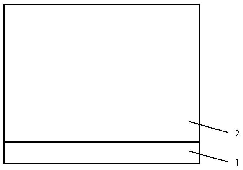
[0067] Step a: The N- epitaxial region 2 is formed by epitaxial growth on the N+ substrate region 1, such as Figure 2a Shown.

[0068] First, the thickness is 350μm, the doping concentration is 5×10 18 cm -3 The SiC substrate is cleaned by RCA standard, and then the thickness of the epitaxial growth is 10μm on the N+ substrate area 1, and the doping concentration is 6×10 15 cm -3 的N-extension zone 2.

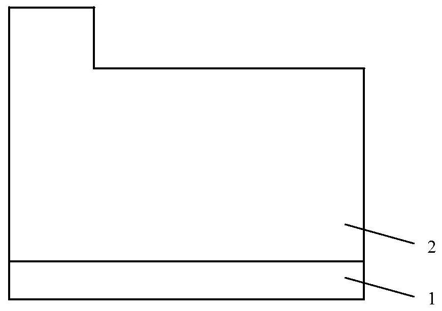
[0069] Step b: Etching to form a thinner N- epitaxial region 2, such as Figure 2b Shown.

[0070] A mask layer is deposited on the upper surface of the N- epitaxial region 2, a mask pattern is formed by a photolithography etching process, and then an ICP etching method is used to etch such as Figure 2b The partial depth of ...


PUM

PropertyMeasurementUnit
Depthaaaaaaaaaa
Widthaaaaaaaaaa
Depthaaaaaaaaaa

Abstract

The invention relates to a silicon carbide UMOSFET device integrated with a TJBS. The device comprises an N+ substrate region, an N- epitaxial region, a P-well region, an N+ injection region, first P+injection regions, second P+ injection regions, a grid electrode, a source electrode and a drain electrode, wherein the second P+ injection regions and the first P+ injection regions are arranged atintervals and are consistent in depth; first grooves are formed in the first P+ injection regions; second grooves are formed in the second P+ injection regions, the depth of the grid electrode is larger than that of the P-well region and smaller than these of the first P+ injection regions, the source electrode forms ohmic contact with the interfaces of the P-well region, the N+ injection region,the first P+ injection regions and the second P+ injection regions, and forms Schottky contact with the interface of the N-epitaxial region. According to the device, a groove structure is introducedinto a Schottky diode structure integrated in the device, so that the depths of the first P+ injection regions and the second P+ injection regions are increased, P+ injection is carried out on the surface of a thinner N-epitaxial region formed through etching, the depths of the P+ injection regions are larger, and the avalanche resistance of the device is improved.

Description

technical field [0001] The invention belongs to the technical field of semiconductors, and in particular relates to a silicon carbide UMOSFET device integrating TJBS. Background technique [0002] In recent years, with the continuous development of power electronic systems, higher requirements have been placed on the power devices in the system. Silicon (Si)-based power electronic devices have been unable to meet the requirements of system applications due to the limitations of the material itself. As a representative of the third-generation semiconductor material, silicon carbide (SiC) materials are far better than silicon materials in many characteristics. Silicon carbide MOSFET (Metal-Oxide-Semiconductor Field-Effect Transistor, Metal-Oxide-Semiconductor Field-Effect Transistor) device, as a commercialized device in recent years, has an alternative in terms of on-resistance, switching time, switching loss and heat dissipation performance. The huge potential of the existi...

Claims


Application Information

Patent Timeline
IPC IPC(8): H01L29/78H01L21/336H01L29/06H01L29/16H01L29/423
CPCH01L29/0603H01L29/0684H01L29/1608H01L29/4236H01L29/66068H01L29/7827H01L29/7839
Inventor 汤晓燕余意何艳静袁昊宋庆文张玉明
Owner 芜湖西晶微电子科技有限公司
Why Eureka
Try Eureka