A silicon carbide umosfet device with integrated jbs
A silicon carbide and device technology, used in semiconductor devices, semiconductor/solid-state device manufacturing, electrical components, etc., can solve the problem of weak internal freewheeling capability of silicon carbide UMOSFET devices, increasing the complexity and cost of circuit systems, and incapable of device freewheeling. and other problems, to achieve the effects of improving breakdown characteristics, reducing manufacturing costs, and improving freewheeling capability.
- Summary
- Abstract
- Description
- Claims
- Application Information
AI Technical Summary
Problems solved by technology
Method used
Image
Examples
Embodiment 1
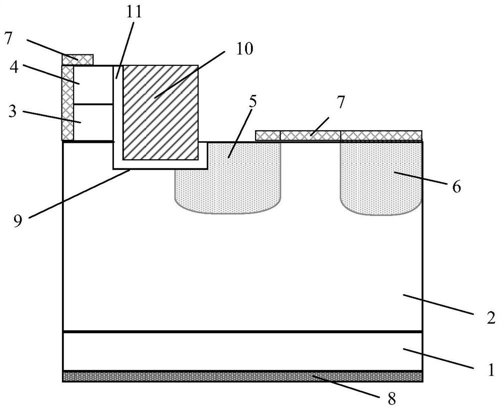
[0034] See figure 1 , figure 1 It is a schematic structural diagram of a silicon carbide UMOSFET device integrating JBS (Junction Barrierschottky, Junction Barrier Schottky) provided by an embodiment of the present invention. As shown in the figure, the silicon carbide UMOSFET device integrating JBS in the embodiment of the present invention includes:
[0035] N+ substrate region 1;
[0036] The N- epitaxial region 2 is arranged on the N+ substrate region 1;
[0037] The P-well region 3 is arranged on the N-epitaxial region 2;
[0038] The N+ injection region 4 is arranged on the P-well region 3;
[0039] The first P+ implantation region 5 is located inside the N- epitaxial region 2;
[0040] The second P+ implantation region 6 is located inside the N- epitaxial region 2 and is spaced apart from the first P+ implantation region 5;
[0041] The gate is arranged adjacent to the P-well region 3 and the N+ implantation region 4, and is partially located inside the N-epitaxy ...
Embodiment 2
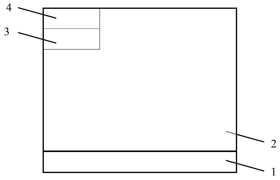
[0059] See Figure 2a-Figure 2h , Figure 2a-Figure 2h It is a process schematic diagram of a silicon carbide UMOSFET device integrating JBS provided by an embodiment of the present invention, and the preparation method includes the following steps:
[0060] Step a: Form N- epitaxial region 2 on N+ substrate region 1 by means of epitaxial growth, such as Figure 2a shown.
[0061] First, the thickness is 350 μm, and the doping concentration is 5×10 18 cm -3 The SiC substrate was cleaned by RCA standard, and then epitaxially grown on the N+ substrate region 1 with a thickness of 10 μm and a doping concentration of 6×10 15 cm -3 N-Epi region 2.
[0062] Step b: Perform well implantation on the upper surface of the N- epitaxial region 2 to form a P-well region 3, and perform N ion implantation in the P-well region 3 to form an N+ implantation region 4, such as Figure 2b shown.
[0063] Deposit and form a mask layer on the N-epitaxial region 2, form a mask pattern by phot...
PUM
| Property | Measurement | Unit |
|---|---|---|
| depth | aaaaa | aaaaa |
| width | aaaaa | aaaaa |
| depth | aaaaa | aaaaa |
Abstract
Description
Claims
Application Information
 - R&D
- Intellectual Property
- Life Sciences
- Materials
- Tech Scout
- Unparalleled Data Quality
- Higher Quality Content
- 60% Fewer Hallucinations
Browse by: Latest US Patents, China's latest patents, Technical Efficacy Thesaurus, Application Domain, Technology Topic, Popular Technical Reports.
© 2025 PatSnap. All rights reserved.Legal|Privacy policy|Modern Slavery Act Transparency Statement|Sitemap|About US| Contact US: help@patsnap.com


