Structure and fabricating method to make a cell with multi-self-alignment in split gate flash

Inactive Publication Date: 2005-03-24
TAIWAN SEMICON MFG CO LTD
View PDF11 Cites 2 Cited by
  • Summary
  • Abstract
  • Description
  • Claims
  • Application Information

AI Technical Summary

Benefits of technology

[0010] It is a primary objective of the invention to provide a split gate flash cell with self-aligned bit contact to word line, self aligned word line to floating gate and self aligned source line to floating gate. It is also a primary objective of the invention to provide a method of forming a split gate flash cell with self-aligne

Problems solved by technology

In arriving at the design rule the possibility of misalignment must be taken into account, which results in a required separation well beyond that needed to avoid development of shorts.
This requirement for i

Method used


Image

  • Structure and fabricating method to make a cell with multi-self-alignment in split gate flash
  • Structure and fabricating method to make a cell with multi-self-alignment in split gate flash
  • Structure and fabricating method to make a cell with multi-self-alignment in split gate flash

Examples


Example

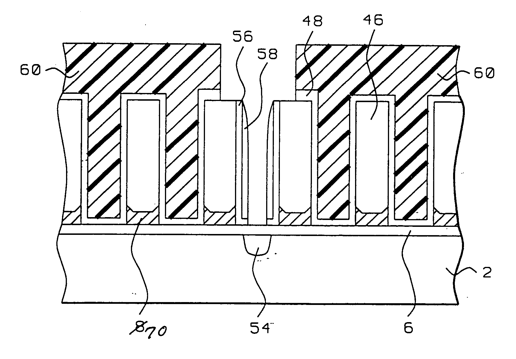
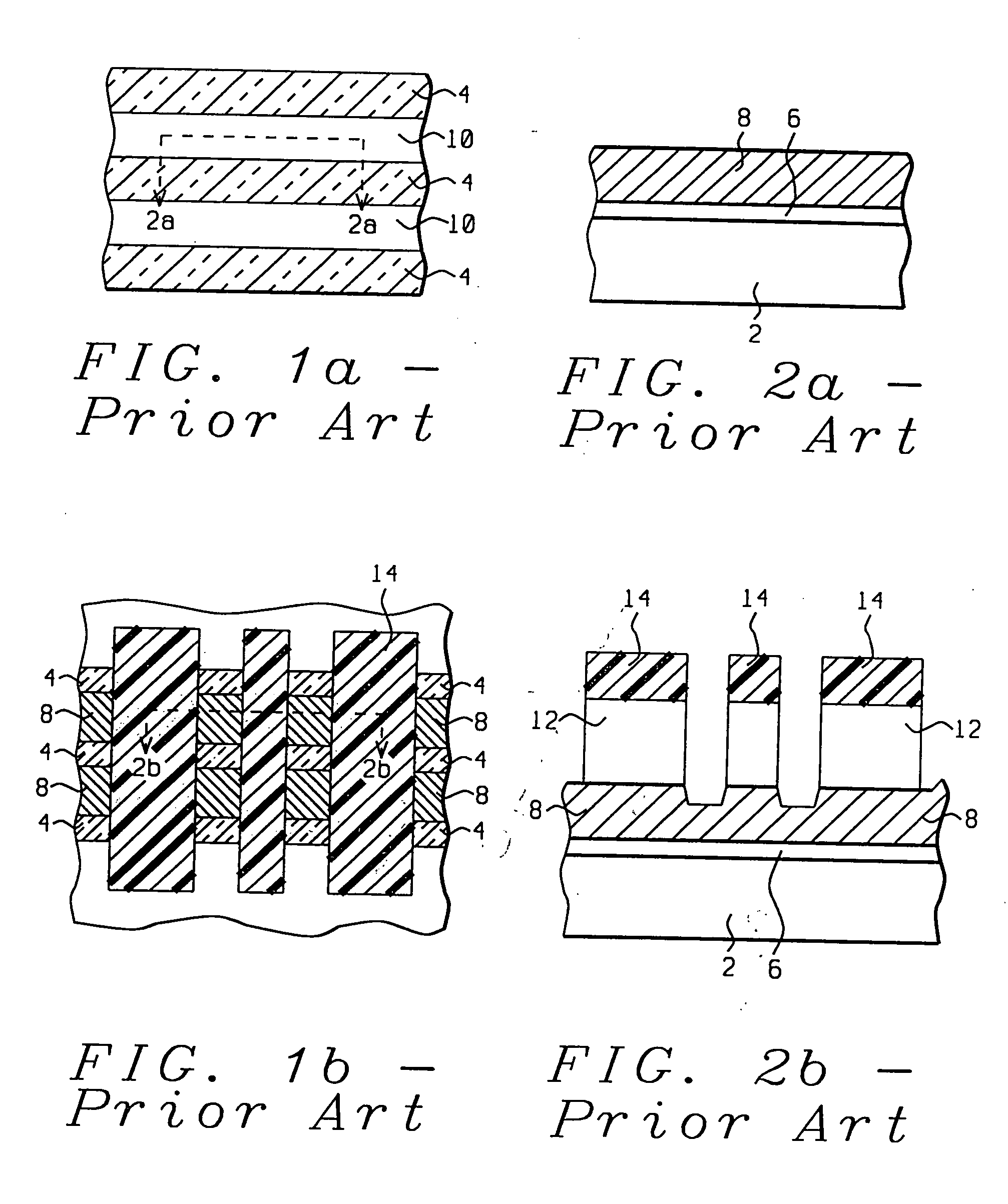
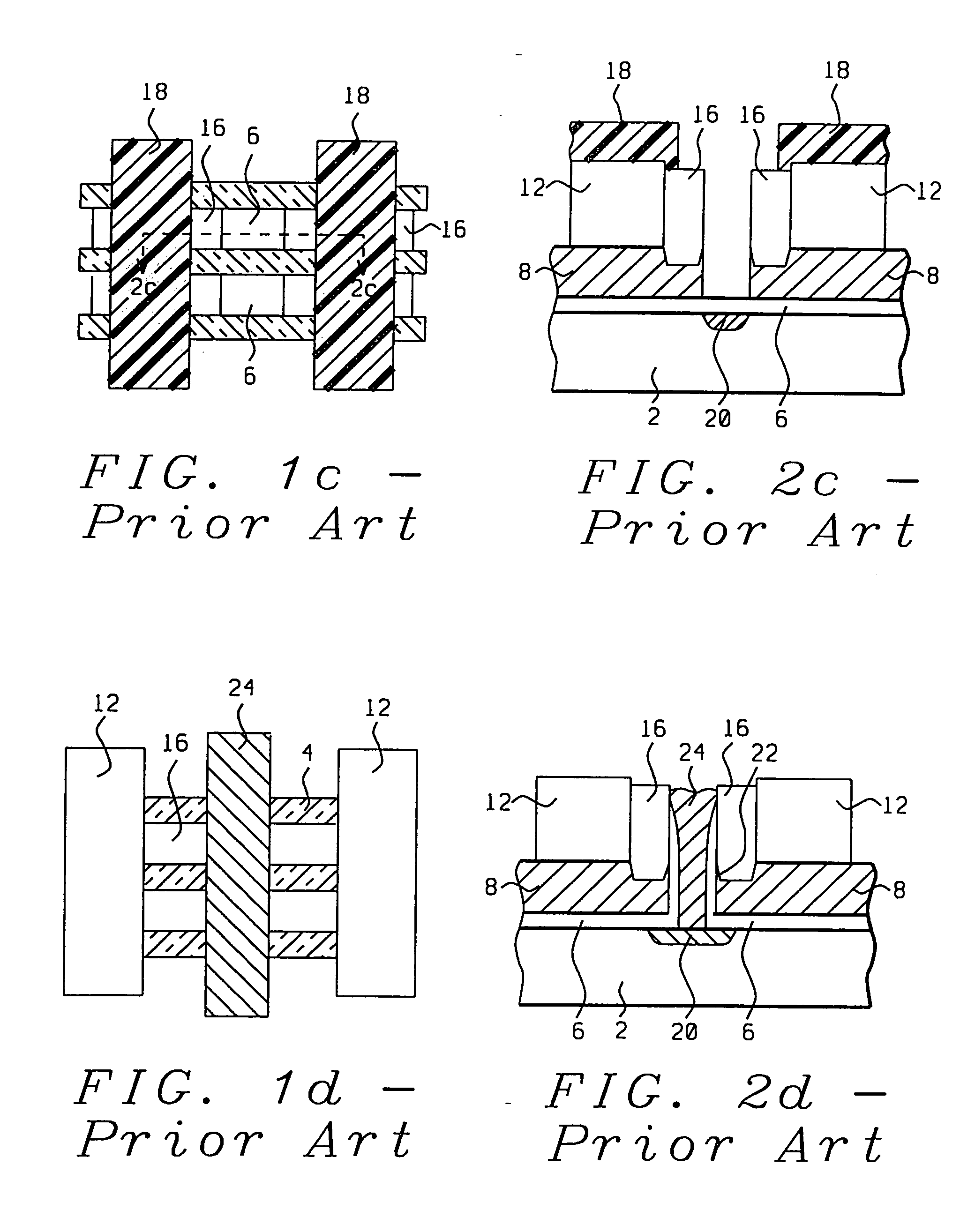
[0019] Preferred embodiments of the invention are well described with the aid of FIGS. 3a-3g and 4a-4g. A method of fabricating a novel split gate flash memory cell is presented in FIGS. 3a-3g, where top views of the cell are presented at successive stages of the process and in FIGS. 4a-4g, which show the corresponding cross-sections. A floating gate insulator layer, 6, which preferably is an oxide layer is formed on a semiconductor region, 2, which preferably is a silicon region, to a thickness of about 80 Angstroms, followed by deposition of a first conductor layer, 8, which preferably is a doped poly 1 layer, to a depth of about 800 Angstroms. The doped poly 1 layer, and also the subsequent doped poly layers, is preferably phosphorus doped either in situ or by ion implantation to achieve a high conductivity. Active regions, 10, are defined using isolating regions, such as shallow trench isolation regions, 4. This is followed by deposition of a first insulator layer, which prefera...


PUM


Abstract

A new structure for split gate flash memory devices is disclosed with multi-self-alignment. Active regions, arranged in rows, are disposed over a semiconductor region and separated by isolation regions. Split gate memory cells are arranged in identical order along the rows of active regions, each memory cell being composed of four elements: drain, word line, floating gate and source elements denoted by D, W, F and S respectively, which are arranged as . . . DWFSFWDWFSFWD . . . so that drain elements, which adjoin word elements on either side, and source elements, which adjoin floating gate elements on either side, are each shared by two memory cells. Floating gate elements are composed of a gate insulator layer disposed over the semiconductor region, conductive floating gates disposed over the gate insulator layer, an insulator layer disposed over the floating gates, and sidewall insulator layers. Source elements, self aligned to said adjoining floating gate elements, are composed of source regions, contained within the semiconductor region, extending below the adjoining floating gate elements, with conductive source pick up lines disposed over and electrically connected to the source regions and which electrically connect corresponding source regions of all rows, and with a source element insulator layer disposed over the source pick up lines. Word line elements, self aligned to floating gate elements on one side and drain elements on the other side, are composed of a word line gate insulator layer disposed over the semiconductor region, with conductive word lines disposed over the word line gate insulator that connect corresponding word line elements of all rows, with a word line insulator layer disposed over the word lines and with word line sidewall insulator layers on side walls facing drain regions. Drain elements, self aligned to said adjoining word line elements, are composed of drain regions, contained within the semiconductor region, with conductive drain pick up lines disposed over and electrically connected to the drain regions and which electrically collect all drain regions for each row.

Description

BACKGROUND OF THE INVENTION [0001] (1) Field of the Invention [0002] The present invention relates generally to semiconductor integrated circuit technology and more particularly to split gate memory cells used in flash EPROMs (Electrically Erasable Programmable Read Only Memory). [0003] (2) Description of Prior Art [0004] Increased performance in computers is often directly related to a higher level of circuit integration. Tolerances play an important role in the ability to shrink dimensions on a chip. Self-alignment of components in a device serves to reduce tolerances and thus improve the packing density of chips. Other techniques can be important in shrinking device size. A method is disclosed later in the embodiments of the present invention of forming a structure with self-aligned source to floating gate, word line to floating gate and bit line contact to word line, which allows for significant reduction in the area of the split gate flash cell. [0005] As is well known in the a...

Claims


Application Information

Patent Timeline
IPC IPC(8): H01L21/8247H01L27/115H01L29/423
CPCH01L27/115H01L29/42324H01L27/11521H10B69/00H10B41/30
Inventor HSIEH, CHIA-TA
Owner TAIWAN SEMICON MFG CO LTD
Why Eureka
Try Eureka