Self-align planerized bottom electrode phase change memory and manufacturing method

a technology of phase change memory and bottom electrode, which is applied in the direction of thermoelectric device junction materials, semiconductor devices, electrical equipment, etc., can solve the problems of short time between a top electrode and a bottom electrode, and the manufacturing of such devices with very small dimensions

Active Publication Date: 2007-07-12
MACRONIX INT CO LTD
View PDF99 Cites 197 Cited by
  • Summary
  • Abstract
  • Description
  • Claims
  • Application Information

AI Technical Summary

Benefits of technology

[0011] The present invention describes a method for aligning a bottom electrode member in a phase change random access memory PCRAM device where a top electrode member serves as a mask for self-align etching of the bottom electrode member. The sides of the bottom electrode member are in alignment with the sides of the top electrode member. The bottom electrode has a top surface that is planarized by chemical mechanical polishing. The top electrode also has a top surface that is planarized by chemical mechanical polishing. A bottom electrode layer like TiN is formed over a substrate prior to the formation of a via during subsequent process steps. A first dielectric layer is formed over the b

Problems solved by technology

Problems have arisen in manufacturing such devices with very small dimensions, and with variations in process that meet tight specifications needed for large-scale memory

Method used


Image

  • Self-align planerized bottom electrode phase change memory and manufacturing method
  • Self-align planerized bottom electrode phase change memory and manufacturing method
  • Self-align planerized bottom electrode phase change memory and manufacturing method

Examples


Embodiment Construction

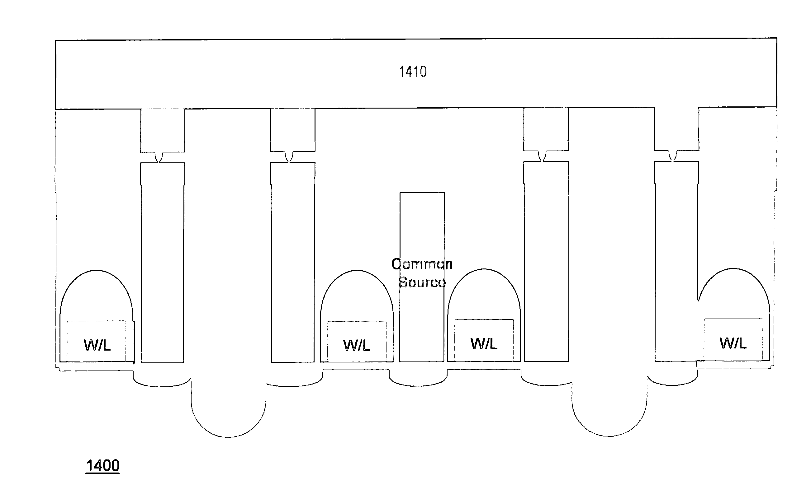
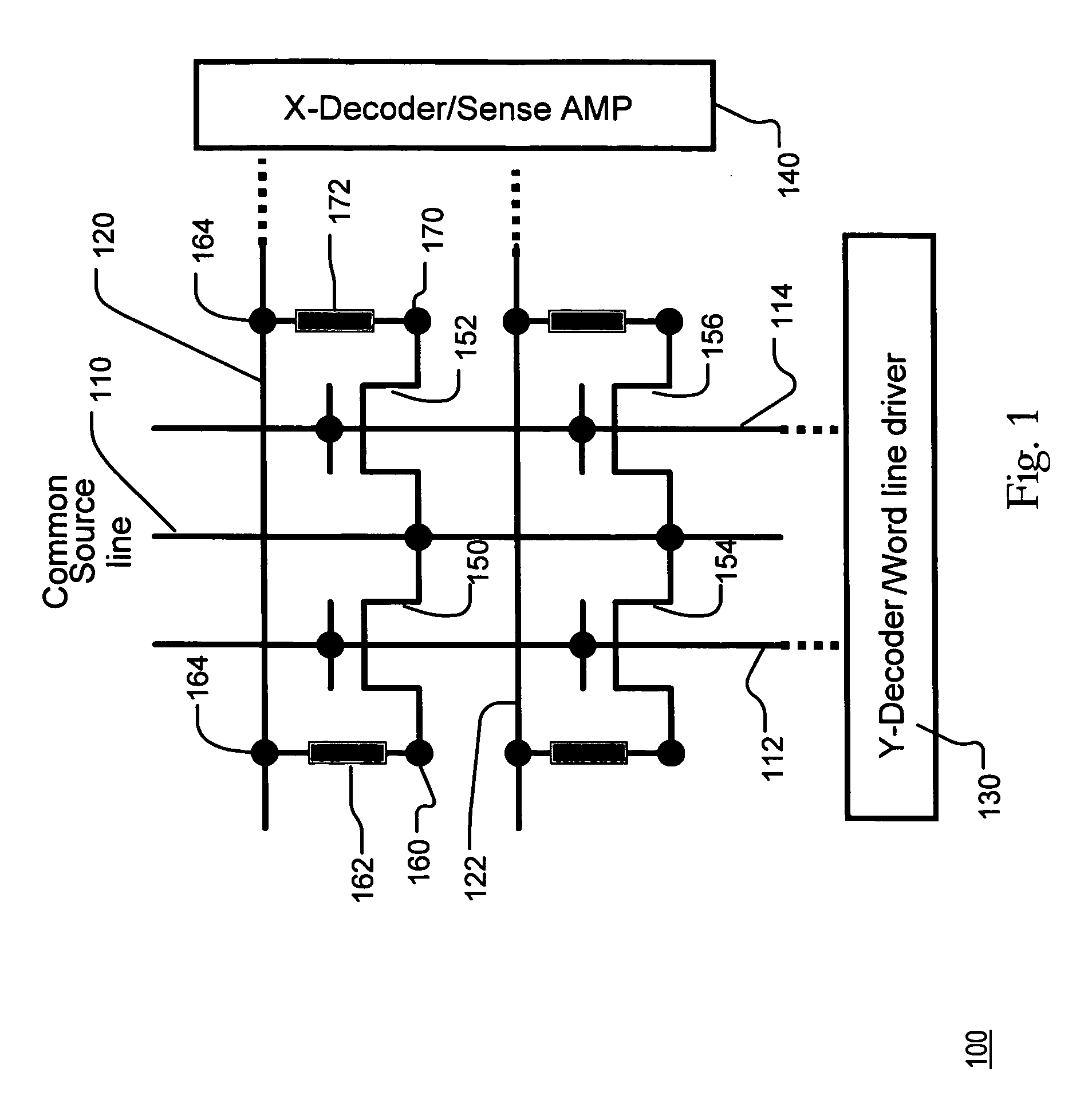
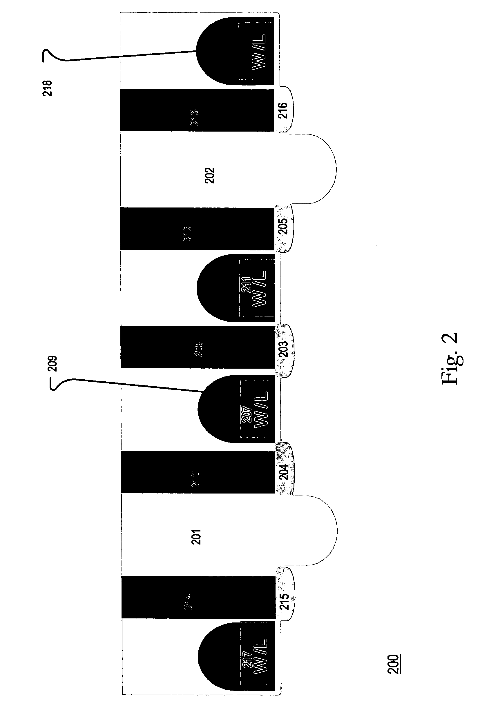
[0030] A description of embodiments of the present invention is provided with reference to FIGS. 1-14.

[0031] Referring now to FIG. 1, there is shown a structure illustrating a memory array 100 comprising phase change memory elements. A common source line 110, a word line 112 and a word line 114 are arranged generally parallel in the Y-direction. Bit lines 120 and 122 are arranged generally parallel in the X-direction. A Y-decoder and a word line driver in block 139 are coupled to the word lines 112, 114. An X-decoder and a set of sense amplifiers in block 140 are coupled to the bit lines 120 and 122. The common source line 110 is coupled to the source terminals of access transistors 150, 152, 154 and 156. The gate of access transistor 150 is coupled to the word line 112. The gate of access transistor 152 is coupled to the word line 114. The gate of access transistor 154 is coupled to the word line 112. The gate of access transistor 156 is coupled to the word line 114. The drain of ...


PUM


Abstract

A method is described for self-aligning a bottom electrode in a phase change random access memory PCRAM device where a top electrode serves as a mask for self-aligning etching of the bottom electrode. The bottom electrode has a top surface that is planarized by chemical mechanical polishing. The top electrode also has a top surface that is planarized by chemical mechanical polishing. A bottom electrode layer like TiN is formed over a substrate and prior to the formation of a via during subsequent process steps. A first dielectric layer is formed over the bottom electrode layer, and a second dielectric layer is formed over the first dielectric layer. A via is formed at a selected section that extends through the first and second dielectric layers.

Description

RELATED APPLICATION DATA [0001] The benefit of U.S. Provisional Patent Application No. 60 / 757,933, filed 11 Jan. 2006, entitled SELF-ALIGN PLANARIZED BOTTOM ELECTRODE PHASE CHANGE MEMORY AND MANUFACTURING METHOD, is hereby claimed.Parties to a Joint Research Agreement [0002] International Business Machines Corporation, a New York corporation; Macronix International Corporation, Ltd., a Taiwan corporation, and Infineon Technologies A.G., a German corporation, are parties to a Joint Research Agreement. BACKGROUND OF THE INVENTION [0003] 1. Field of the Invention [0004] The present invention relates to high density memory devices based on phase change based memory materials, including chalcogenide based materials and other materials, and to methods for manufacturing such devices. [0005] 2. Description of Related Art [0006] Phase change based memory materials are widely used in read-write optical disks. These materials have at least two solid phases, including for example a generally am...

Claims


Application Information

Patent Timeline
IPC IPC(8): H01L29/08
CPCH01L45/06H01L45/1233H01L45/126H01L45/143H01L27/2436H01L45/1246H01L45/148H01L45/1691H01L45/144H10B63/30H10N70/828H10N70/8413H10N70/8825H10N70/884H10N70/231H10N70/068H10N70/8828H10N70/826
Inventor LUNG, HSIANG-LAN
Owner MACRONIX INT CO LTD
Why Eureka
Try Eureka