Phase Change Memory Cell and Manufacturing Method

a phase change memory and manufacturing method technology, applied in semiconductor devices, digital storage, instruments, etc., can solve the problems of manufacturing such devices with very small dimensions, and achieve the effect of small phase change structure and greater thermal conductivity of the higher reset transition temperature portion

Active Publication Date: 2007-06-28
MACRONIX INT CO LTD
View PDF99 Cites 208 Cited by
  • Summary
  • Abstract
  • Description
  • Claims
  • Application Information

AI Technical Summary

Benefits of technology

[0011] A first embodiment of a phase change memory cell made according to the present invention includes first and second electrodes and a phase change element electrically coupling the first and second electrodes. At least a section of the phase change element comprises a higher reset transition temperature portion and a lower reset transition temperature portion. The lower reset transition temperature portion comprises a phase change region which can be transitioned, by the passage of electrical current therethrough, from generally crystalline to generally amorphous states at a lower temperature than the higher reset transition temperature portion. According to some embodiments the phase change element comprises an outer, generally tubular portion surrounding an inner portion, the outer portion comprising a higher reset transition temperature portion and the inner portion comprising a lower reset transition temperature portion. With some embodiments the thermal conductivity of the higher reset transition temperature portion is greater than the thermal conductivity of the lower reset transition temperature portion when both are in generally crystalline states.
[0012] One example for making a phase change memory cell carried out according to the present invention proceeds as follows. First and second electrodes are electrically coupled with a phase change element, the phase change element comprising phase change material. The coupling step comprises pr

Problems solved by technology

Problems have arisen in manufacturing such devices with very small dimensions, and with va

Method used


Image

  • Phase Change Memory Cell and Manufacturing Method
  • Phase Change Memory Cell and Manufacturing Method
  • Phase Change Memory Cell and Manufacturing Method

Examples


Embodiment Construction

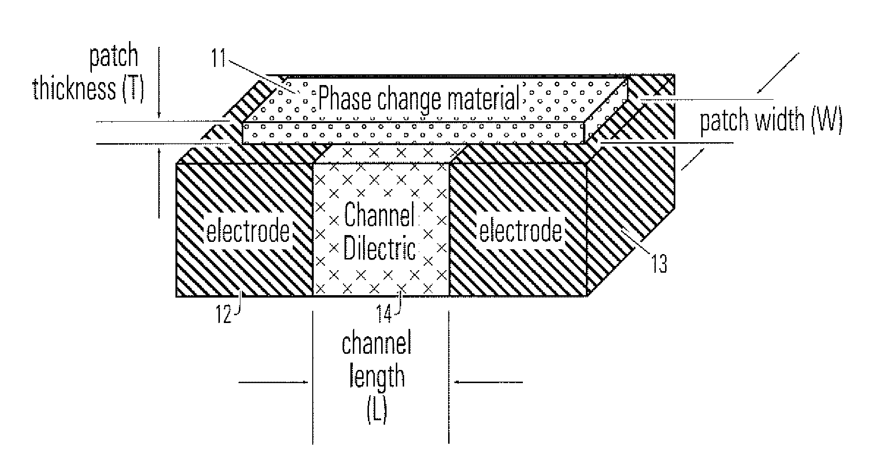
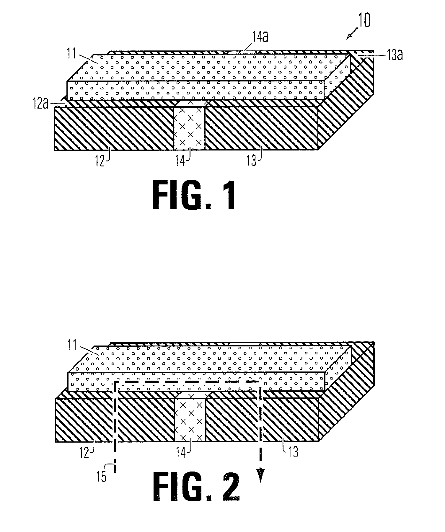
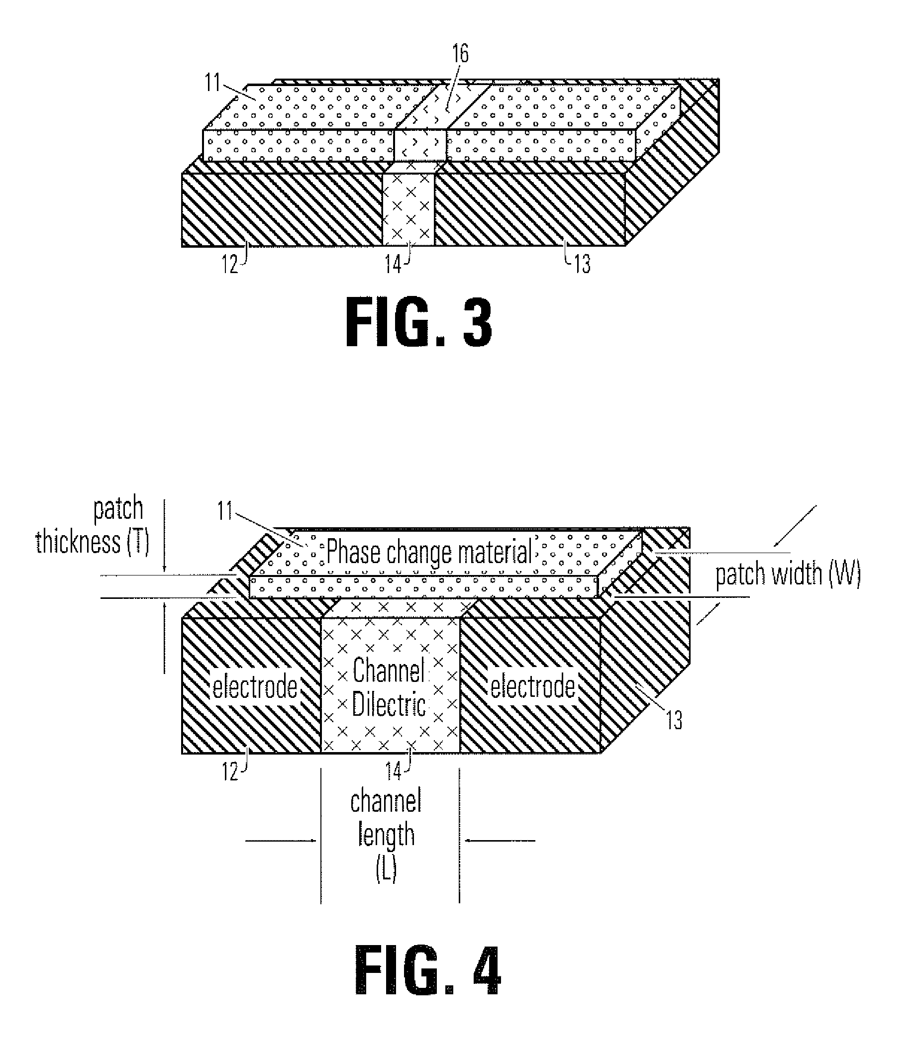
[0057] A detailed description of thin film fuse phase change memory cells, arrays of such memory cells, and methods for manufacturing such memory cells, is provided with reference to FIGS. 1-23. The embodiments of the invention of FIGS. 24-31 are a first set of examples of phase change memory cells having higher and lower reset transition temperature portions. The embodiment of the invention of FIGS. 32-41 is a second example of a phase change memory cell having a phase change element with higher and lower reset transition temperature portions.

[0058] The following description of the invention will typically be with reference to specific structural embodiments and methods. It is to be understood that there is no intention to limit the invention to the specifically disclosed embodiments and methods but that the invention may be practiced using other features, elements, methods and embodiments. Like elements in various embodiments are commonly referred to with like reference numerals....


PUM


Abstract

A phase change memory cell includes first and second electrodes electrically coupled by a phase change element. At least a section of the phase change element comprises a higher reset transition temperature portion and a lower reset transition temperature portion. The lower reset transition temperature portion comprises a phase change region which can be transitioned, by the passage of electrical current therethrough, from generally crystalline to generally amorphous states at a lower temperature than the higher reset transition temperature portion. The phase change element may comprise an outer, generally tubular, higher reset transition temperature portion surrounding an inner, lower reset transition temperature portion.

Description

CROSS-REFERENCE TO RELATED APPLICATIONS [0001] This application claims the benefit of U.S. provisional patent application No. 60 / 752,138 entitled Phase Change Memory Cell and Manufacturing Method, filed on 19 Dec. 2005, Attorney Docket No. MXIC 1686-1. This application is a continuation in part of U.S. patent application Ser. No. 11 / 424,177 entitled Phase Change Memory Cell and Manufacturing Method, filed on 14 Jun. 2006, Attorney Docket No. MXIC 1665-2, which application claims the benefit of U.S. provisional patent application No. 60 / 740,176 entitled Phase Change Memory Cell and Manufacturing Method, filed on 28 Nov. 2005, Attorney Docket No. MXIC 1665-1.BACKGROUND OF THE INVENTION [0002] 1. Field of the Invention [0003] The present invention relates to high density memory devices based on phase change based memory materials, including chalcogenide based materials and other materials, and to methods for manufacturing such devices. [0004] 2. Description of Related Art [0005] Phase ...

Claims


Application Information

Patent Timeline
IPC IPC(8): G11C11/00
CPCG11C8/08G11C8/10G11C13/0004G11C13/0028G11C2213/79H01L27/2436H01L27/2463H01L45/06H01L45/1226H01L45/1233H01L45/143H01L45/144H01L45/148H01L45/1625H01L45/165H01L45/1675G11C2213/53H10B63/30H10B63/80H10N70/231H10N70/823H10N70/826H10N70/8825H10N70/884H10N70/8828H10N70/043H10N70/026H10N70/063
Inventor LUNG, HSIANG-LANLIU, RICHCHEN, SHIH-HUNGCHEN, YI-CHOU
Owner MACRONIX INT CO LTD
Why Eureka
Try Eureka