Output gain stage for a power amplifier

a power amplifier and gain stage technology, applied in differential amplifiers, amplifiers with semiconductor devices/discharge tubes, amplifier details, etc., can solve the problems of large parasitic capacitance, difficult fabrication, and significant area consumed by pmos devices, and achieve the effect of small capacitan

Active Publication Date: 2010-08-03
AVAGO TECH INT SALES PTE LTD
View PDF25 Cites 36 Cited by
  • Summary
  • Abstract
  • Description
  • Claims
  • Application Information

AI Technical Summary

Problems solved by technology

As a result, a significant amount of area is consumed by the PMOS devices and a correspondingly large parasitic capacitance is created.
In turn, this requires a relatively small inductance to resonate out this capacitance, which can be difficult to fabricate.
Furthermore, the larger PMOS devices present a larger non-linear gate capacitance that can adversely affect linearity of the PA.

Method used


Image

  • Output gain stage for a power amplifier
  • Output gain stage for a power amplifier
  • Output gain stage for a power amplifier

Examples


Embodiment Construction

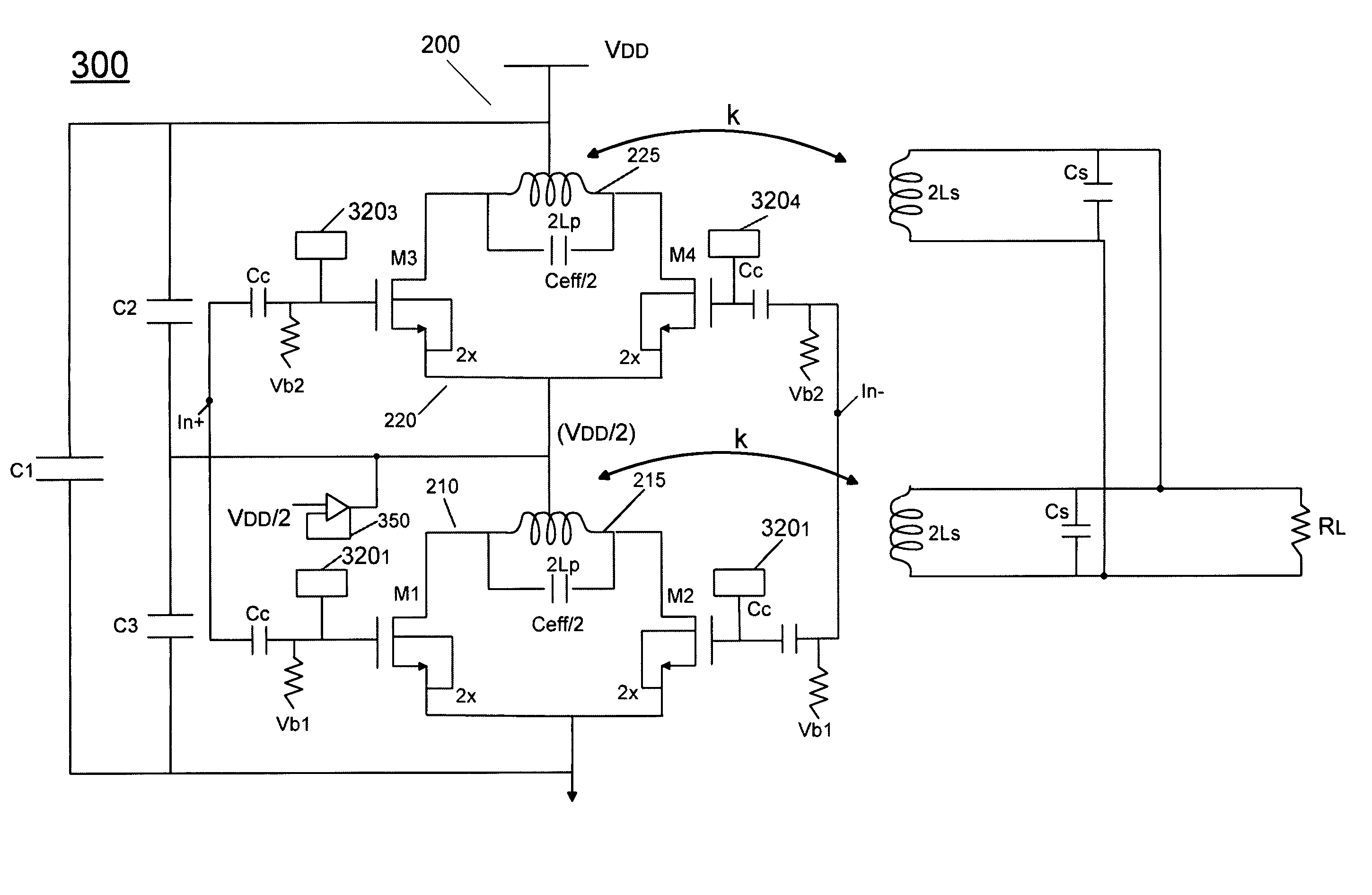
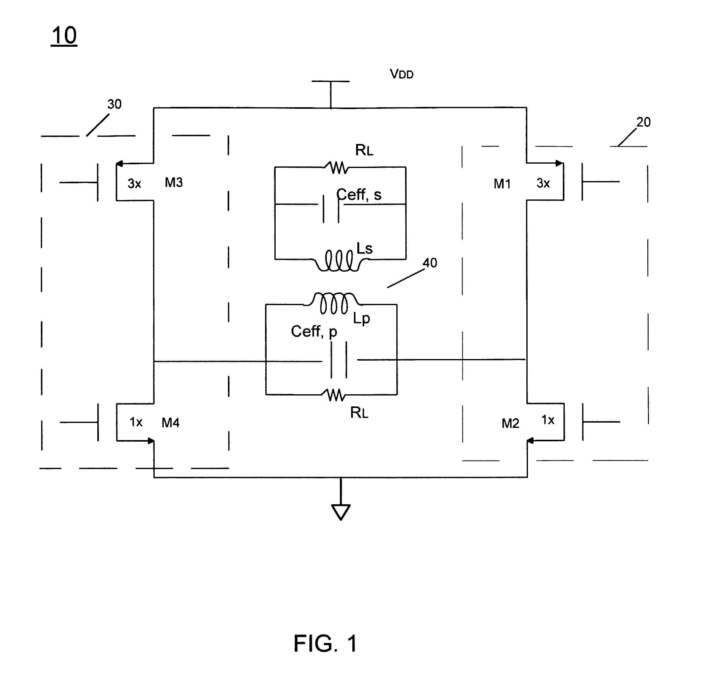
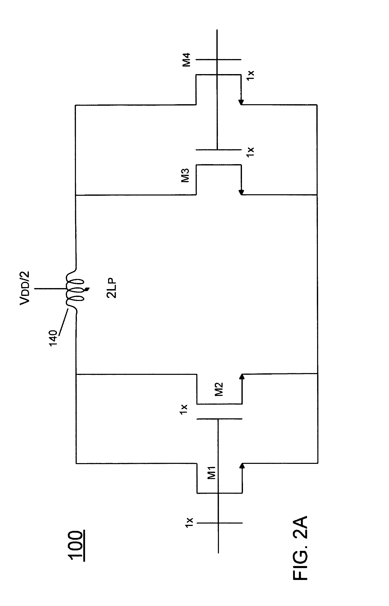
[0018]Embodiments may provide an output gain stage that is formed without PMOS devices. That is, an output gain stage for a PA implemented in a CMOS process technology (instead of a GaAs process technology), can be formed using only NMOS gain devices such as NMOS transconductors. As used herein, the term “CMOS PA” refers to such a PA that is formed via a CMOS process. As will be described below, such a PA may include multiple gain stages and / or driver stages formed using both PMOS and NMOS devices. However, in various embodiments, at least an output gain stage may be formed using only NMOS devices. Because of the size difference between NMOS and PMOS devices, replacing the PMOS devices with higher ft NMOS devices leads to a reduced area for the transistors and a corresponding reduction in total effective capacitance, i.e., parasitic capacitance. Further, by reducing parasitic capacitance, the non-linear effects caused by the parasitic capacitance are also reduced, easing implementat...


PUM


Abstract

In one embodiment, the present invention includes multiple gain stages to receive and amplify a differential input signal at different common mode voltages. The stages each may include a pair of linear NMOS gain transistors coupled to a primary coil of a given output transformer. One of the stages may include commonly coupled terminals coupled to a center tap of the primary coil of an output transformer of another stage, and a supply current provided to one of the stages is re-used for the other stage(s).

Description

BACKGROUND[0001]Power amplifiers (PAs) are commonly used in wireless devices to amplify a signal for transmission. PAs are typically formed of multiple stages, and often include a final gain stage, commonly referred to as an output gain stage, to amplify the signal to a desired power level for its output to a load such as an antenna that radiates the amplified signal.[0002]Wireless communication systems dictate the amount of power to be output. Different requirements may exist in different communication protocols. Many communication systems have various requirements for a handset to achieve with relation to power, efficiency, and linearity over varying signal levels. For example, a variety of communication systems, including enhanced data rates for GSM evolution (EDGE), long term evolution (LTE / 4 G), WiFi in accordance with an IEEE 802.11 standard, worldwide interoperability for microwave access (WiMax), code division multiple access (CDMA), and wideband-code division multiple acces...

Claims


Application Information

Patent Timeline
Patent Type & Authority Patents(United States)
IPC IPC(8): H03F3/45
CPCH03F3/211H03F3/45183H03F2200/537
Inventor SRINIVASAN, VISHNUBOCKELMAN, DAVID E.
Owner AVAGO TECH INT SALES PTE LTD
Why Eureka
Try Eureka