
Reduced mask count gate conductor definition

a technology of mask count and conductor, applied in the field of semiconductor device fabrication, can solve the problems of not all structures being formed, photolithographic techniques becoming inability to reliably create structures of the dimensions required, and the size of semiconductor devices has decreased

Inactive Publication Date: 2010-08-10
GLOBALFOUNDRIES INC
View PDF9 Cites 2 Cited by
  • Summary
  • Abstract
  • Description
  • Claims
  • Application Information

AI Technical Summary

Problems solved by technology

As the size of semiconductor devices has decreased, photolithographic techniques become unable to reliably create structures of the dimensions required.
However, SIT methods produce structures, usually hard masks, of generally closed-loop geometry.
Furthermore, not all structures being formed are to be of the same small dimensions typically produced by SIT methods.

Method used


Image

  • Reduced mask count gate conductor definition
  • Reduced mask count gate conductor definition
  • Reduced mask count gate conductor definition

Examples


Embodiment Construction

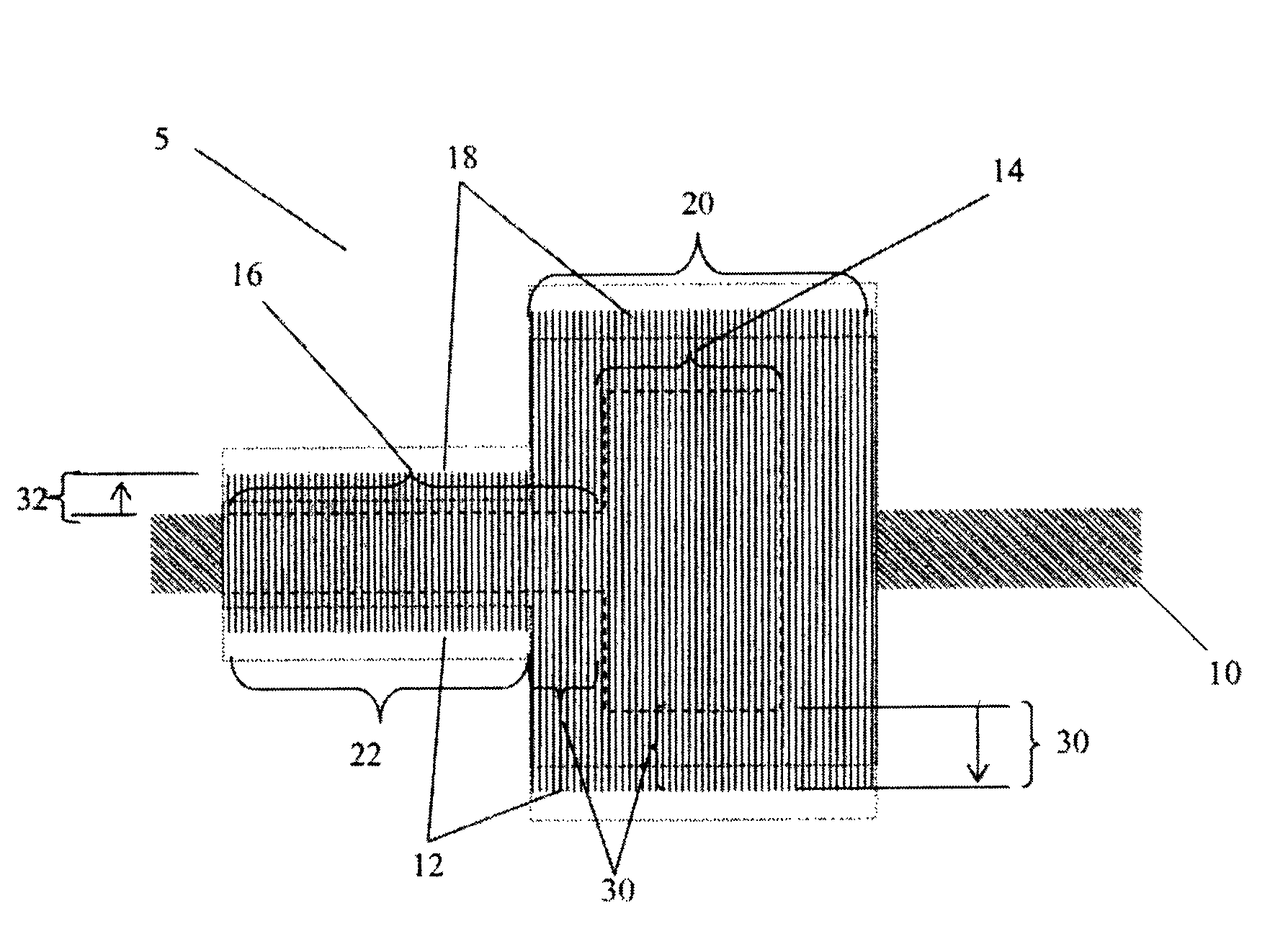
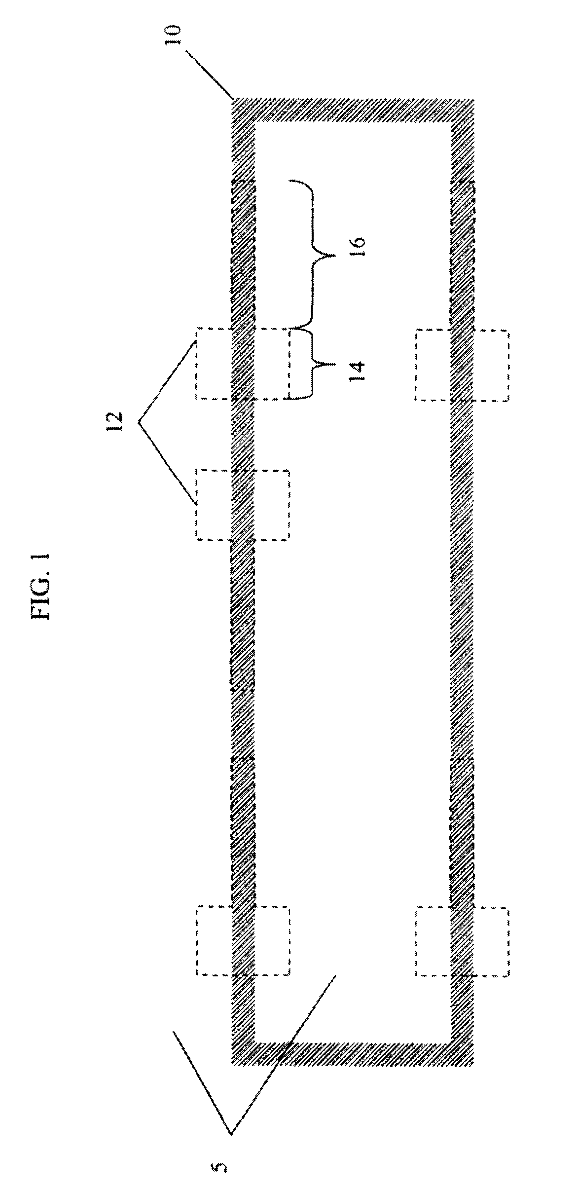
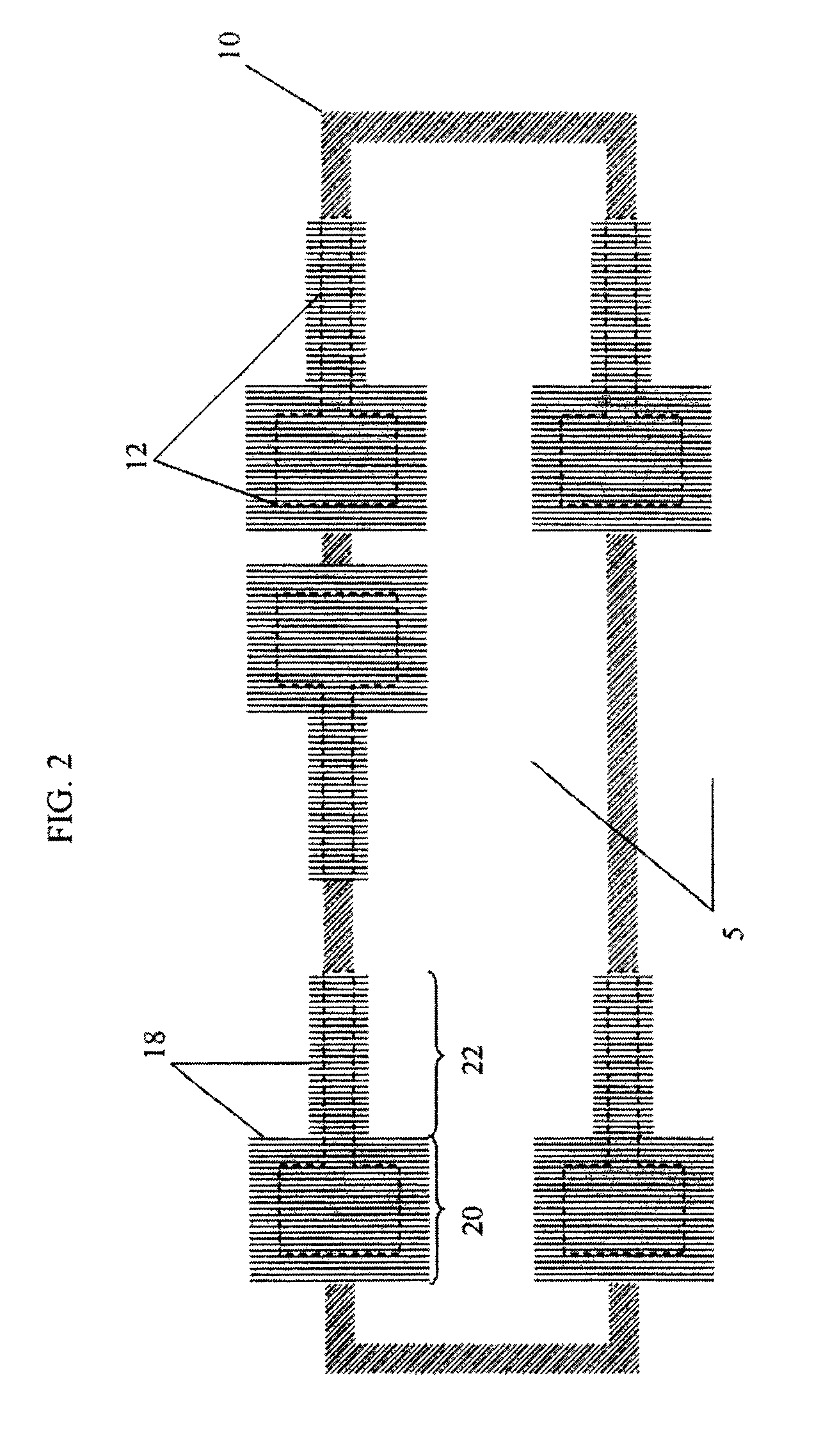
[0015]The invention relates to semiconductor fabrication, and more particularly to fabricating a combination of small and large structures. In embodiments of the invention, a reduction in the number of masks required to form a final image especially when combining SIT imaging processes with traditional masking techniques is possible. In one embodiment, the method of the invention generally includes, for example, forming a follow-on mask over a section of a sidewall image transfer (SIT) loop on a substrate for further imaging the underlying substrate. The follow-on mask enables cutting the loop into segments and adds larger features to the image formed by the SIT loop, without interfering with the accuracy for those portions of the final image formed by the SIT loop.

[0016]Referring to FIG. 1, a hard mask 10 image in the form of a SIT loop built using SIT-related techniques is shown. Although a hard mask loop 10 is shown, any imaging technique which builds a continuous, single-width l...


PUM

PropertyMeasurementUnit
semiconductoraaaaaaaaaa
widthaaaaaaaaaa
critical widthaaaaaaaaaa

Abstract

A combined wide-image and loop-cutter pattern is provided for both cutting and forming a wide-image section to a hard mask on a substrate formed by sidewall imaging techniques in a reduced number of photolithographic steps. A single mask is formed which provides a wide mask section while additionally providing a mask to protect the critical edges of an underlying hard mask during hard mask etching. After the hard mask is cut into sections, the protective portions of the follow-on mask are removed to expose the critical edges of the underlying hard mask while maintaining shapes necessary for defining wide-image sections. Thus, the hard mask cutting, hard mask critical edge protecting, and large area mask may be formed in a reduced number of steps.

Description

FIELD OF THE INVENTION[0001]The invention relates to semiconductor fabrication, and more particularly to fabricating a combination of small and large structures.BACKGROUND DESCRIPTION[0002]As the size of semiconductor devices has decreased, photolithographic techniques become unable to reliably create structures of the dimensions required. As photolithographic techniques have become unusable, other technologies have been developed to create the small structures required by the ever shrinking semiconductor devices. One example of a non-photolithographic imaging technique is sidewall image transfer (“SIT”).[0003]SIT is able to produce structures substantially narrower than the minimum size achievable with photolithographic techniques, while maintaining excellent width control. However, SIT methods produce structures, usually hard masks, of generally closed-loop geometry. These loops have a single, well-controlled width (referred to henceforth as the “critical image width”). Convention...

Claims


Application Information

Patent Timeline
Patent Type & Authority Patents(United States)
IPC IPC(8): B44C1/22C03C15/00C03C25/68C23F1/00
CPCH01L21/0337H01L21/0338H01L21/32139
Inventor FURUKAWA, TOSHIHARUHAKEY, MARK C.HOLMES, STEVEN J.HORAK, DAVID V.KOBURGER, III, CHARLES W.
Owner GLOBALFOUNDRIES INC
Learn More