Power supply unit

a power supply unit and power supply technology, applied in the direction of power supply lines, dc-dc conversion, power conversion systems, etc., can solve the problems of inability to achieve the ic cost, circuits and the like for realizing the remaining phases, and the like in the like of the associated on-resistance power loss and heat generation, etc., to achieve the effect of low cos

Inactive Publication Date: 2010-08-17
RENESAS ELECTRONICS CORP
View PDF6 Cites 14 Cited by
  • Summary
  • Abstract
  • Description
  • Claims
  • Application Information

AI Technical Summary

Benefits of technology

[0008]In such a buck converter, a switching-type buck converter providing a high power-efficiency is typically used. If the switching type is used, then a reduction in the ripple voltage generated by switching, support for higher current, and the like become important. That is, for the latter case, as the amount of load current increases, the associated on-resistance related power loss and heat generation and the like of the switching transistor cannot be neglected. In order to solve such problems, for example, as described in Patent Documents 1, 2, and non-Patent Document 1, a multiphase technique is advantageously used, in which a plurality of inductors is in parallel connection with a common capacitor, and a current is fed through each of the inductors in a different phase. If the multiphase technique is used, then, in principle, the more the number of phases, the further the ripple voltage will be reduced. Moreover, since the amount of load current may be supplied in a distributed manner from each inductor (each switching transistor), coping with higher current becomes easy. Moreover, since the inductor's value can be reduced, a higher speed can be also achieved.
[0009]However, if the techniques of Patent Documents 1, 2, and non-Patent Document 1 are used, it is necessary to always provide a master IC (the phase control device of Patent Document 1, the control IC of Patent Document 2, the control IC of non-Patent Document 1) and to couple a plurality of slave ICs thereto. Therefore, a lower cost cannot be achieved in terms of the mounting area, the IC cost, and the like. For example, in realizing a multiphase power supply having fewer phases than six phases by using the technique of non-Patent Document 1, the circuits and the like for realizing the remaining phases will be wasted. On the other hand, for example, if the techniques of Patent Documents 1, 2 are used, slave ICs corresponding to the number of phases desired to realize may be provided, however, a master IC always needs to be additionally provided. Therefore, especially the fewer the number of phases to realize, the further the cost performance will decrease. In particular, since the mounting area is limited in a notebook PC or various mobile computing devices, the interconnect wires for the mounted component and between the mounted components are preferably reduced as much as possible.
[0010]It is thus one of the objects of the present invention to provide a power supply unit capable of realizing a multiphase power supply at low cost. In addition, the above-described object and other objects and the novel features of the present invention will be apparent from the description of the present specification and the accompanying drawings.
[0013]If such a configuration is used, a master IC as in the prior art needs not to be provided, and therefore the multiphase power supply operation can be realized at low cost. Note that, more specifically, in order to realize the multiphase power supply operation with such a configuration, any one of a plurality of semiconductor devices needs to generate a trigger pulse signal only once during startup, for example. Then, each of the semiconductor devices includes a function to generate the trigger pulse signal during the startup depending on setting from the outside. This setting from the outside may be carried out depending on, for example, whether or not an external resistor is coupled to the first input terminal or the first output terminal. This can reduce the number of terminals as compared with the case where a dedicated terminal is provided separately, and thus a low cost can be achieved.
[0014]Moreover, preferably each semiconductor device described above includes an error amplifier circuit for setting the switching time of a transistor, and further includes a second output terminal that outputs an error amplifier signal from this error amplifier circuit, and a second input terminal that can also receive an error amplifier signal from other than itself. This allows, for example, any one of the semiconductor devices to generate an error amplifier signal and allows other semiconductor devices to share this error amplifier signal. Since this can reduce the number of wirings and the like, a lower cost can be achieved, and moreover, since the setting criterion of the switching time in each of the semiconductor devices is the same, a switching control having a small variation for each phase can be carried out. In addition, in particular, if a peak current control method is used in carrying out this switching control, the current for each phase can be equalized easily, which is beneficial. In this case, furthermore, by detecting a current for each phase by the current of a transistor within each semiconductor device, the number of wirings and the like can be reduced as compared with the case where the current of an inductor is detected, and thus a lower cost can be achieved.
[0016]To briefly describe the effect obtained by the representative invention among the inventions disclosed in the present application, multiphase power supplies can be realized at low cost.

Problems solved by technology

That is, for the latter case, as the amount of load current increases, the associated on-resistance related power loss and heat generation and the like of the switching transistor cannot be neglected.
Therefore, a lower cost cannot be achieved in terms of the mounting area, the IC cost, and the like.
For example, in realizing a multiphase power supply having fewer phases than six phases by using the technique of non-Patent Document 1, the circuits and the like for realizing the remaining phases will be wasted.
Therefore, especially the fewer the number of phases to realize, the further the cost performance will decrease.

Method used


Image

  • Power supply unit
  • Power supply unit
  • Power supply unit

Examples


embodiment 1

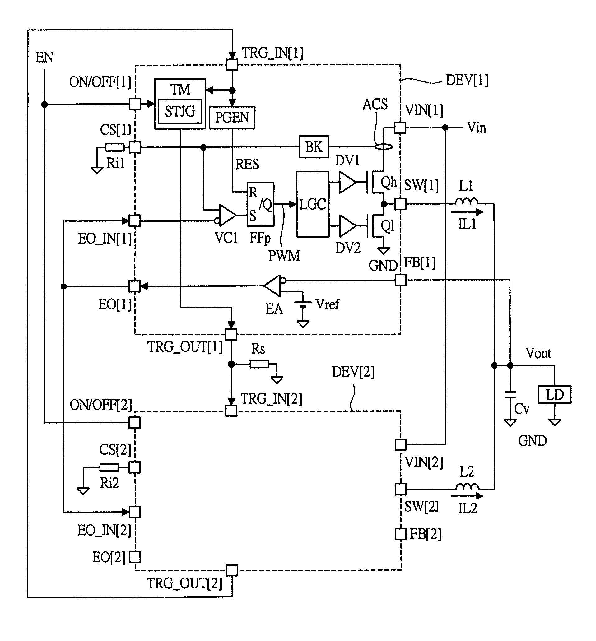
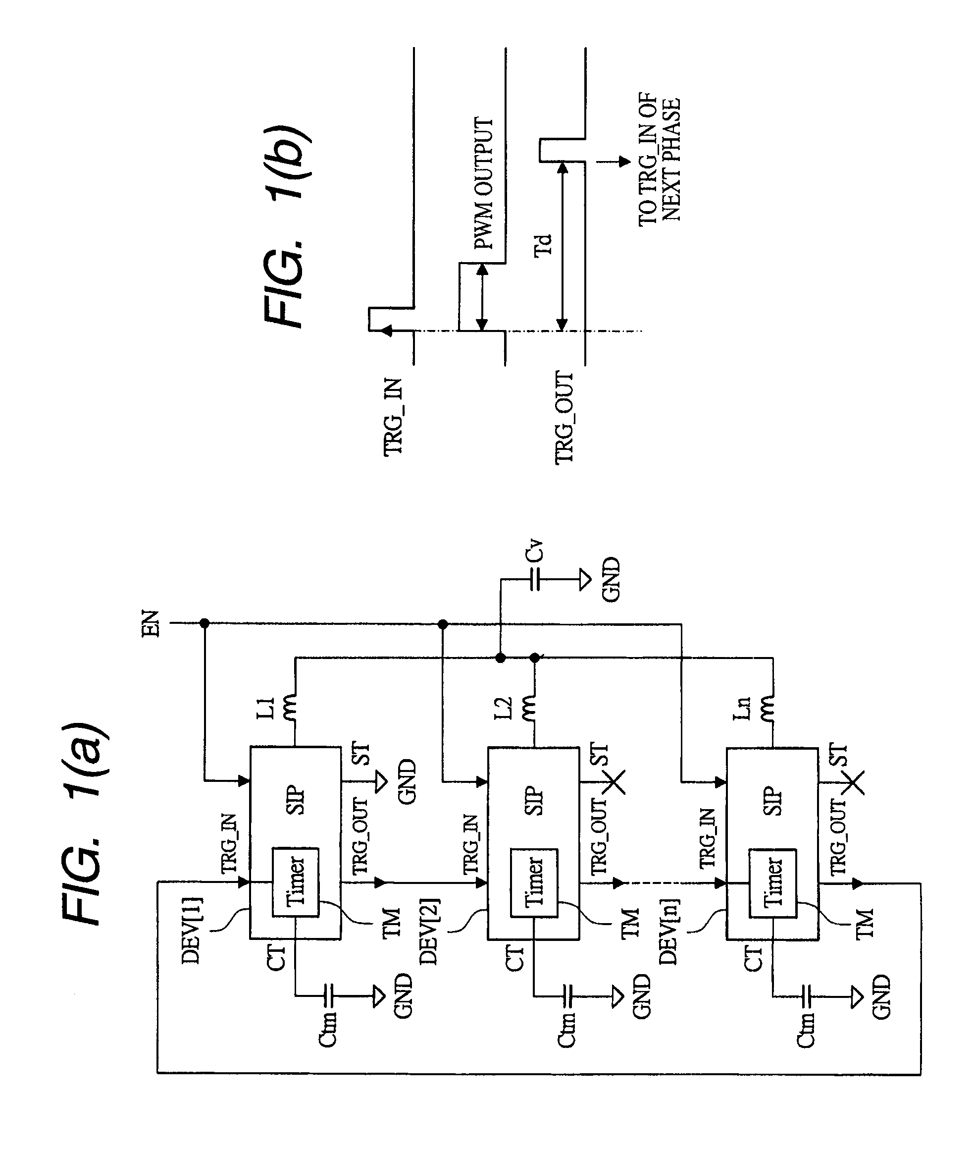
[0032]FIGS. 1(a) and 1(b) show a basic concept of a power supply unit according to Embodiment 1 of the present invention, wherein FIG. 1(a) is a schematic diagram showing a configuration example thereof, and FIG. 1(b) is an explanatory view showing an operation example of FIG. 1(a). The power supply unit shown in FIG. 1(a) has a configuration for realizing a multiphase power supply of n (n>=2) phases, and comprises n semiconductor devices (or semiconductor ICs) DEV[1]-DEV[n], n inductors L1-Ln, an output capacitor Cv, and the like.

[0033]Each of DEV[1]-DEV[n] comprises a trigger input terminal TRG_IN, a trigger output terminal TRG_OUT, and a timer circuit TM. TM receives a signal of TRG_IN as an input, and delays it based on a capacitor Ctm coupled to a delay time setting terminal CT, and outputs the delayed signal from TRG_OUT. Note that, an analog delay based on the capacitor Ctm is used here, but not limited thereto, and this can be replaced with various kinds of generic delay cir...

embodiment 2

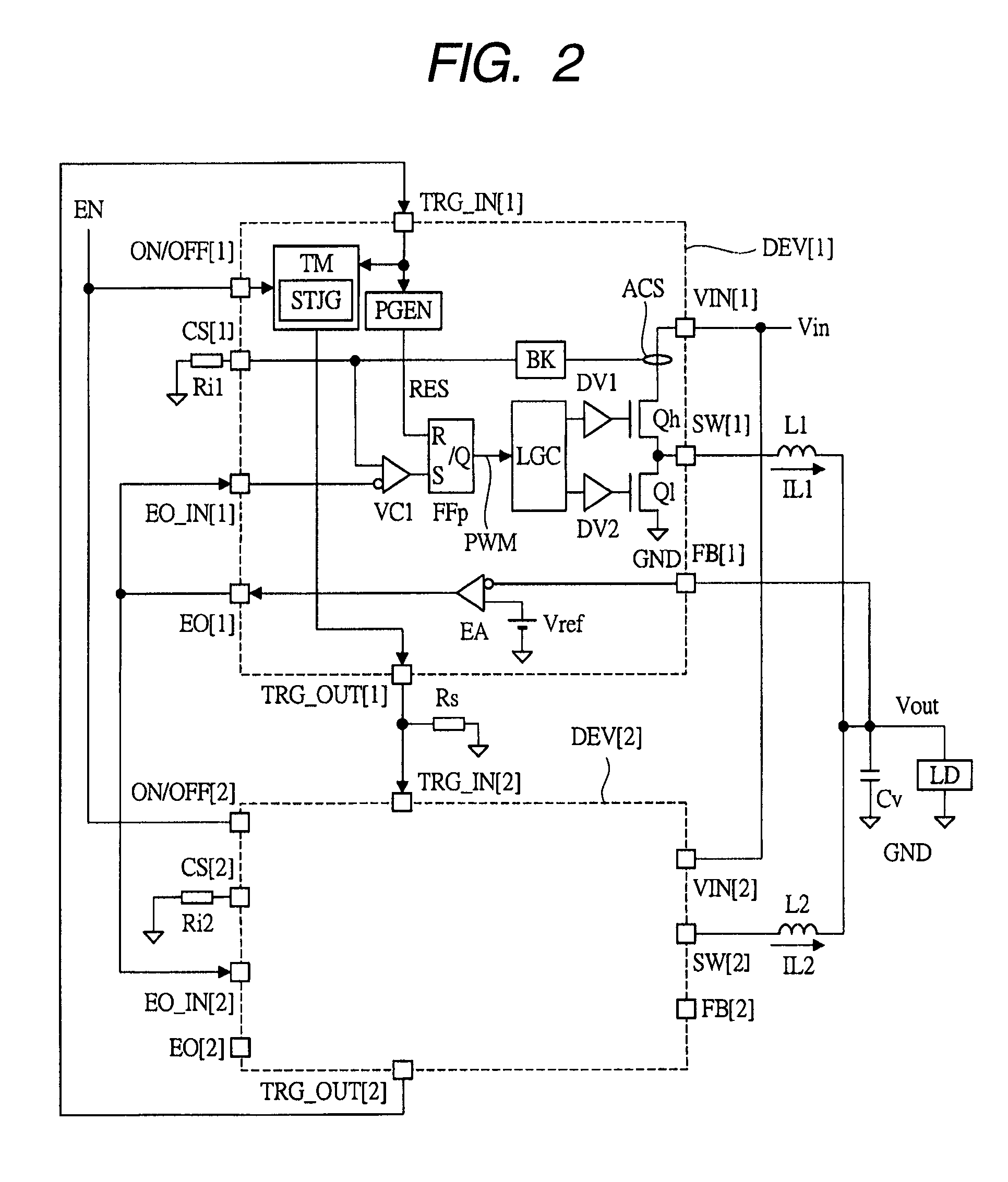
[0052]In Embodiment 2, a more detailed configuration example of the semiconductor device DEV described in Embodiment 1 is described. FIG. 4 is a block diagram showing a detailed configuration example of a semiconductor device used in a power supply unit according to Embodiment 2 of the present invention. FIG. 5 is a plan view showing an example of the package form of the semiconductor device of FIG. 4. The configuration example shown in FIG. 4 is a further embodied one of the configuration example of FIG. 2 described above, and the general configuration and operation thereof are the same as those of FIG. 2 and FIG. 3. Here, the description is made paying attention to the portions further embodied from the configuration example of FIG. 2.

[0053]The semiconductor device (or a semiconductor IC) DEV shown in FIG. 4 basically comprises the transistor Qh serving as a high side transistor (e.g., MOSFET), the transistor Ql serving as a low side transistor (e.g., MOSFET), and various control ...

embodiment 3

[0088]In Embodiment 3, an example is described, in which a single phase power supply is realized using the semiconductor device DEV described in Embodiment 2 (FIG. 4 or the like). FIG. 9 is a wiring diagram showing a configuration example in a power supply unit according to Embodiment 3 of the present invention. To the semiconductor device DEV[1] shown in FIG. 9, the same external resistors and external capacitors as those of DEV of FIG. 4 or DEV[1] of FIG. 6 are coupled. The difference is that the trigger output terminal TRG_OUT of DEV[1] is coupled to its own trigger input terminal TRG_IN, and the external resistor Rs is coupled to this TRG_OUT. Other than this, the configuration is the same as that of DEV of FIG. 4, or DEV[1] of FIG. 6, so the detailed description thereof is omitted.

[0089]Since the semiconductor device DEV described in FIG. 4 or the like does not require a master IC as in the prior art and shows a configuration example capable of operating by itself, it can opera...


PUM


Abstract

To provide a power supply unit capable of realizing a multiphase power supply at low cost. For example, each of a plurality of semiconductor devices DEV[1]-DEV[n] comprises a trigger input terminal TRG_IN, a trigger output terminal TRG_OUT, and a timer circuit TM that delays a pulse signal input from TRG_IN and outputs it to TRG_OUT. DEV[1]-DEV[n] are mutually coupled in a ring shape by its own TRG_IN being coupled to TRG_OUT of one semiconductor device other than itself. Each of DEV[1]-DEV[n] performs switching operation by using the pulse signal from TRG_IN as a starting point, and feeds a current into an inductor L corresponding to itself. Moreover, DEV[1] generates the above-described pulse signal only once during startup by a start trigger terminal ST being set to a ground voltage GND, for example.

Description

CROSS-REFERENCE TO RELATED APPLICATION[0001]The present application claims priority from Japanese patent application No. 2008-57496 filed on Mar. 7, 2008, the content of which is hereby incorporated by reference into this application.BACKGROUND OF THE INVENTION[0002]The present invention relates to a power supply unit, and relates to, for example, a technique effective in application to a switching power supply unit that converts a high voltage into a low voltage.[0003]For example, Patent document 1 (Japanese patent translation publication No. 2005-520475) describes a multiphase buck converter comprising: n inductors in parallel connection with a common capacitor; n output switching devices coupled to these inductors, respectively; n phase output devices that drive these output switching devices by PWM control, respectively; and a phase control device that supplies a common control signal to each of the phase outputting devices (FIG. 1). The phase control device supplies the n phase...

Claims


Application Information

Patent Timeline
Patent Type & Authority Patents(United States)
IPC IPC(8): G05F1/00
CPCH02M3/1584Y10S323/901
Inventor KUDO, RYOTARONAGASAWA, TOSHIO
Owner RENESAS ELECTRONICS CORP
Why Eureka
Try Eureka