Power Amplifier Controller With Polar Transmitter

a power amplifier and transmitter technology, applied in amplifier modifications, baseband system details, wireless communication, etc., can solve the problems of sacrificing more efficiency, reducing overall design complexity, and undesirable wide spectral occupancy, so as to reduce glitches, increase power efficiency, and reduce overall design complexity

Active Publication Date: 2010-12-09
QUANTANCE
View PDF59 Cites 100 Cited by
  • Summary
  • Abstract
  • Description
  • Claims
  • Application Information

AI Technical Summary

Benefits of technology

[0014]Concurrently, the power amplifier controller system both controls an adjustable supply voltage to the PA in an efficient manner, and adjusts the gain of the VGA, based upon an amplitude correction signal generated in an amplitude correction loop. The amplitude correction loop strives to minimize the difference between the amplitude of the output signal and the desired amplitude component generated by the polar modulator, to reduce amplitude distortion. Additionally, the power amplifier controller system may include a phase shifter to adjust the phase of the PA input signal. The phase shifter shifts the phase responsive to a phase correction signal generated in a phase correction loop. The phase correction loop strives to hold constant the phase difference between the phase of the output signal and the phase of the desired phase-modulated component generated by the polar modulator. The phase correction loop corrects for unwanted phase modulation introduced by the AM to PM non-ideality of the power amplifier and thus reduces phase distortion generated by the power amplifier. Advantageously, the power amplifier controller circuit controls the power amplifier so that it operates in an efficient manner while reducing distortion.
[0016]In a second embodiment, a delayed version of the amplitude component and phase modulated signals are compared to the output signal to generate the amplitude correction signal and phase correction signal respectively. The delay compensates for delay through the RF path to reduce glitches caused by misalignment of the signals. Furthermore, a split power supply is used to increase power efficiency. The split power supply comprises a linear regulator and a switched mode power supply to each supply a portion of the PA supply power responsive to different frequency ranges of the amplitude correction signal.
[0017]In a third embodiment, the second embodiment is combined with an alternative phase correction loop that provides the phase correction signal to the polar modulator. The polar modulator shifts the phase of the desired RF signal prior to phase modulation according to the phase correction signal. Thus, the embodiment advantageously eliminates the phase shifter from the RF path and reduces the overall design complexity associated with this phase shifter.

Problems solved by technology

RF PAs are one of the most significant sources of power consumption in these electronic devices, and their efficiency has a significant impact on the battery life on these portable electronic devices.
Since the RF spectrum is shared amongst users of the cellular telephone, a wide spectral occupancy is undesirable.
This typically results in power being wasted during the off-peak of the amplitude of the RF input signal 106, as the biasing remains fixed for the acceptable distortion at the peak power level.
Certain RF modulation techniques have evolved to require even more spectral efficiency, and thereby forcing the RF PA 104 to sacrifice more efficiency.
However, the Large Signal Polar technique often fails to provide significant net efficiency gains, because the supply voltage 109 to the PA 104 cannot be varied in an energy-efficient way to accommodate the large variations in the amplitude signal of the desired RF modulated signal and thus it fails to provide a substantial energy efficiency gain while maintaining the required linear amplification of the RF signal in the RF PA 104.
This is mainly due to the difficulty in realizing a fast, accurate, wide range, and energy efficient voltage converter to drive the supply voltage of the RF PA 104.
Quite often, the conventional methods of controlling a PA fail to address the amplitude-to-phase re-modulation (AM-to-PM) which occurs in a non-frequency linear device such as a PA.
Thus, the conventional methods are not suitable for the common types of PAs for use in common mobile telephony or mobile data systems because the required spectral occupancy performance is compromised by the AM to PM distortion.
Thus, there is a need for an RF PA system that is efficient over a wide variety of modulation techniques and results in a significant net decrease in power consumption by the RF PA circuit.

Method used


Image

  • Power Amplifier Controller With Polar Transmitter
  • Power Amplifier Controller With Polar Transmitter
  • Power Amplifier Controller With Polar Transmitter

Examples


first embodiment

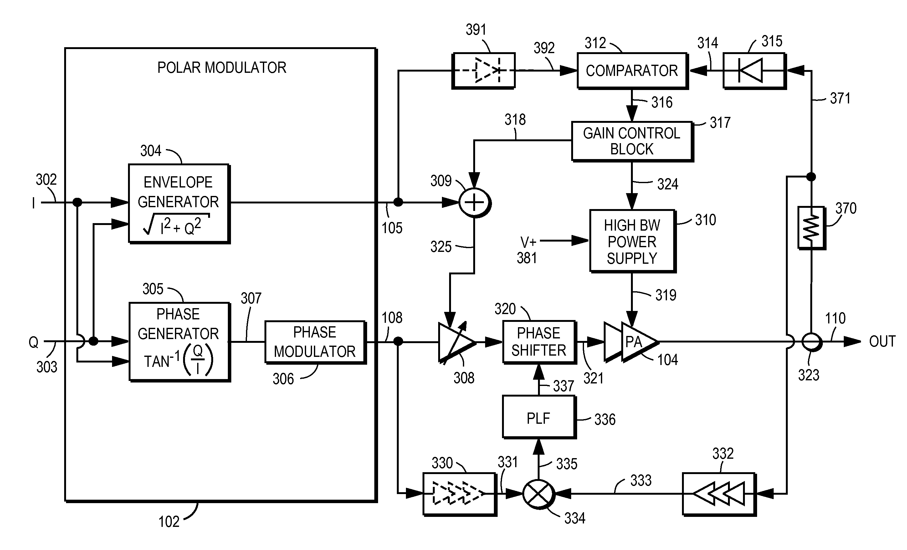
[0029]FIG. 3A illustrates an RF transmitter circuit including a PA controller for operating with a polar modulator 102 according to the present invention. The polar modulator 102 receives I,Q baseband signals 302, 303 and generates an amplitude component 105 of a desired RF signal and a phase modulated signal 108. A variable gain amplifier (VGA) 308 reconstructs the desired RF signal by recombining the phase modulated signal 108 and the amplitude component 105. A power amplifier 104 generates an amplified RF output signal 110 from the reconstructed RF signal 321. Additional circuitry of the PA controller provides feedback control signals that reduce distortion of the RF output signal 110 and increase power efficiency of the PA 104. Operation of the control circuit will be described in further detail below.

[0030]In one embodiment, the polar modulator 102 comprises an envelope generator 304, a phase generator 305, and a phase modulator 306. The envelope generator 304 receives the I,Q ...

second embodiment

[0052]FIG. 4 illustrates an RF transmitter circuit in accordance with the present invention. The circuit in FIG. 4 is similar to the circuit of FIG. 3A with a few variations as will be described. First, delayed versions 346, 344 of the amplitude component 105 and the phase-modulated signal 108 of the desired RF signal are applied to the amplitude and phase correction loops, respectively. In one embodiment, a delay block 301 is inserted between the envelope generator 304 and the comparator 312 in the amplitude correction loop. A delay block 340 in series with another phase modulator 342 is also inserted between the phase generator 305 and the limiter 330 of the phase correction loop. The phase modulator 342 may be a duplicate of the phase modulator 306. Alternatively, the delay block 340 can be inserted after the phase modulator 306 to eliminate the need for the duplicate phase modulator 342. However, a delay block inserted after phase modulator 306 may increase the complexity of the...

third embodiment

[0057]FIG. 5 illustrates yet another RF transmitter circuit in accordance with the present invention. The circuit is similar to the embodiment of FIG. 4 but varies the implementation of the phase correction loop. In this embodiment, the phase shifter 320 in FIG. 4 is eliminated and the output of the VGA 308 is connected directly to the PA input 321. The PLF output 502, which represents the loop phase error, is instead summed with the output of the phase generator 305 at a summer 504, thus providing a pre-shifted phase component 507 to the phase modulator 452. Thus, the phase modulated signal 108 now includes the equivalent phase shifts present after the phase shifter 320 in the embodiments described in FIGS. 3A and 4, but without requiring the phase shifter 320. The embodiment advantageously shifts the phase prior to the phase modulator 452 rather than in the RF path. This removes a potential source of noise and design complexity from the RF signal path.

[0058]In one example, the pha...


PUM


Abstract

A power amplifier controller controls a power amplifier and is coupled to a polar modulator. The polar modulator generates an amplitude component and a phase-modulated component of the desired RF modulated signal, and outputs to the power amplifier controller. The power amplifier controller regenerates a combined phase and amplitude modulated RF signal to generate an input signal to a power amplifier by adjusting the gain of a VGA based on the amplitude component of the desired RF modulated signal. Concurrently, the power amplifier controller both controls an adjusted supply voltage to the PA and adjusts the gain of the VGA based upon an amplitude correction signal or amplitude error signal.

Description

CROSS-REFERENCE TO RELATED APPLICATIONS[0001]This application is a continuation application of, and claims priority under 35 U.S.C. §120 from, U.S. patent application Ser. No. 11 / 858,705, entitled “Power Amplifier Controller with Polar Transmitter,” filed on Sep. 20, 2007, which is incorporated by reference herein in its entirety. This application is related to U.S. patent application Ser. No. 11 / 670,931 entitled “Amplifier Compression Control Circuit” filed on Feb. 2, 2007 and U.S. patent application Ser. No. 11 / 429,119 entitled “Power Amplifier Controller Circuit” filed on May 4, 2006, the entire contents of which are both incorporated by reference herein in their entirety.BACKGROUND OF THE INVENTION[0002]1. Field of the Invention[0003]The present invention relates to a circuit for controlling RF PAs (Radio Frequency Power Amplifiers), and more specifically, to an RF PA controller circuit that operates with a polar transmitter.[0004]2. Description of the Related Art[0005]RF (Radio...

Claims


Application Information

Patent Timeline
Patent Type & Authority Applications(United States)
IPC IPC(8): H04W88/02
CPCH03F1/0222H03F1/0233H03F1/32H03F3/24H04B2001/0425H03F2200/451H03F2200/78H03F2200/99H03F2200/324H03F1/3241
Inventor VINAYAK, VIKASDROGI, SERGE FRANCOISTOMASZ, MARTIN
Owner QUANTANCE
Why Eureka
Try Eureka