

Organic light emitting device
a light-emitting device and organic technology, applied in semiconductor devices, electrical devices, instruments, etc., can solve problems such as inability to display white color properly, and achieve the effect of improving white color balan
- Summary
- Abstract
- Description
- Claims
- Application Information
AI Technical Summary
Benefits of technology
Problems solved by technology
Method used
Image

Examples
first embodiment
[0059]FIG. 4 is a layout illustrating a portion of an OLED according to the invention. FIG. 5 is a cross-sectional view taken along the line I-I′ in FIG. 4. The OLED of the present embodiment has different size driver transistors.
[0060]Referring to FIG. 4, an OLED according to the present embodiment includes a scan line 132, a data line 150, a power supplying line (VDD) 154 and driver transistors. Neighboring driver transistors may have a different size from each other.
[0061]Referring to FIG. 4 and FIG. 5, an insulation layer 107 is formed on a substrate 105. The substrate 105 may be optically transparent. The substrate 105 may include a glass substrate, quartz substrate, glass ceramic substrate and crystallized glass substrate, etc. Preferably, the substrate is made of a material having a heat resisting property.
[0062]The insulation layer 107 is efficient for a substrate including ions moving in the substrate, or a substrate that is electrically conductive. When the substrate is a ...
third embodiment
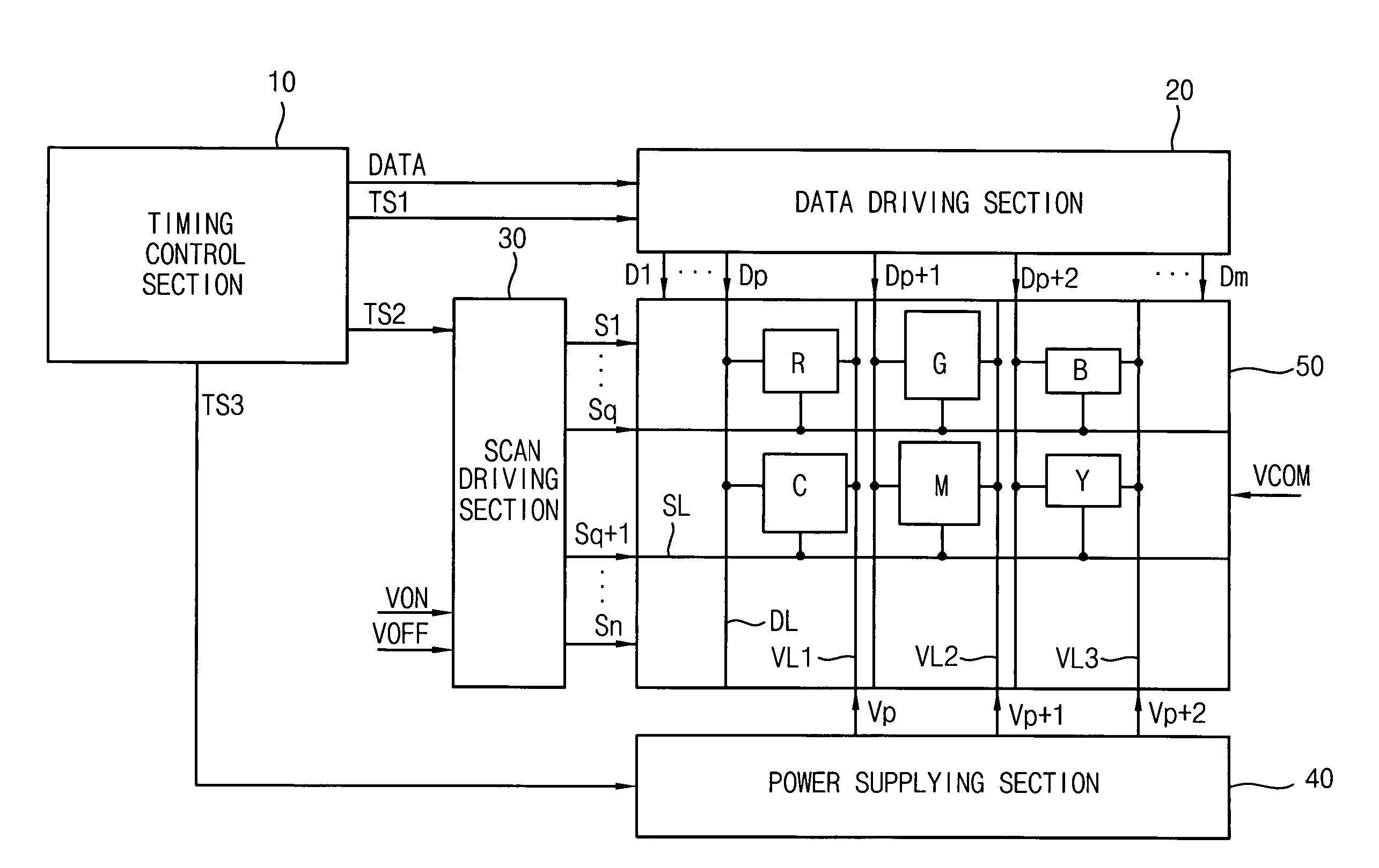
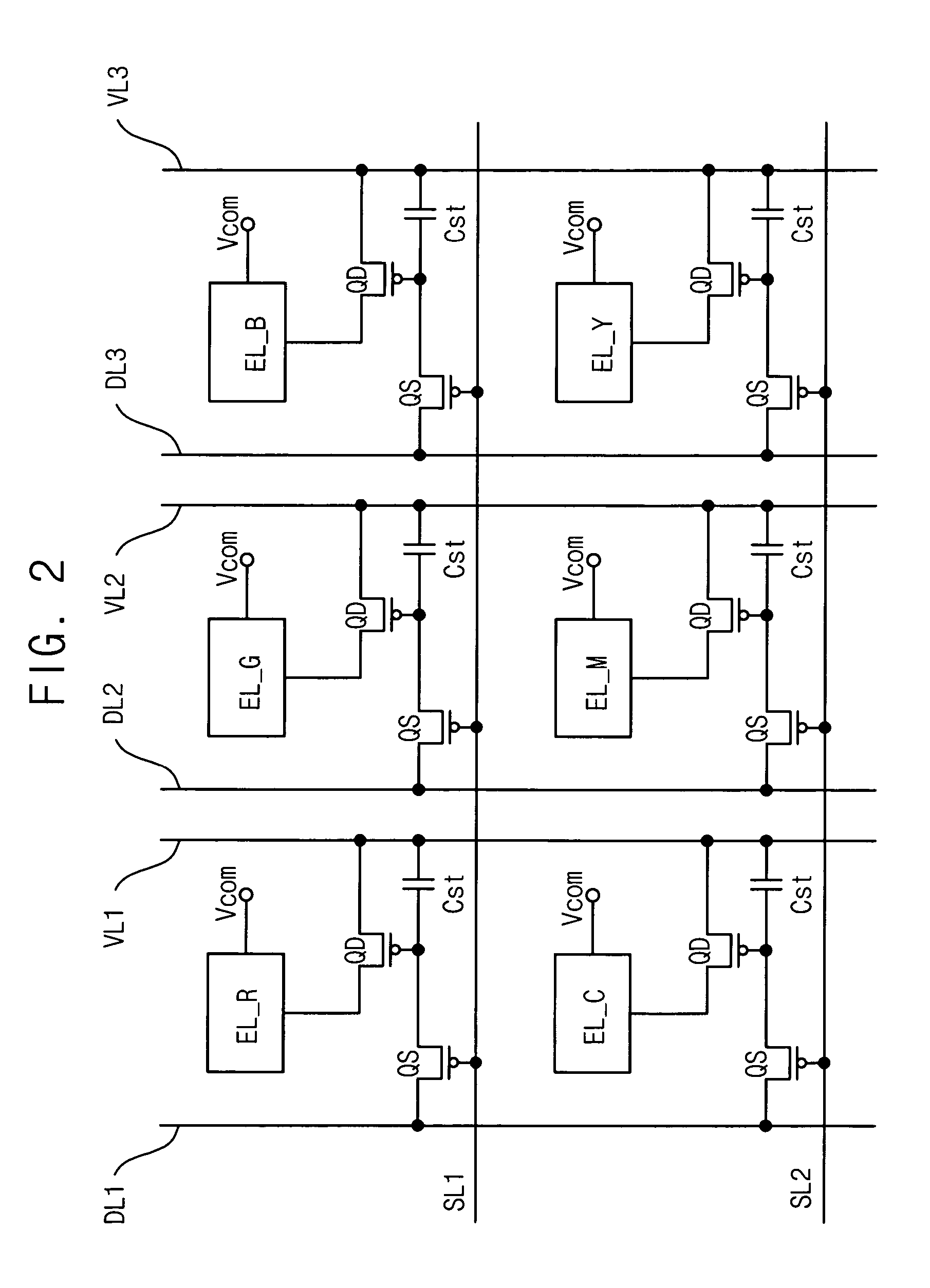
[0121]FIG. 17 is a schematic block diagram illustrating an OLED according to the invention. In a non-limiting embodiment, the OLED includes pixels arranged in a three by two matrix shape and applied with bias voltages of different magnitude.
[0122]Referring to FIG. 17, the OLED includes a timing control section 210, a data driving section 220, a scan driving section 230, a power supplying section 240, and an organic light emitting panel 250.
[0123]The timing control section 210 receives an image signal DATA and control signal from an external graphic controller (not shown) to generate first, second and third timing signals TS1, TS2 and TS3. The timing control section 210 provides the data driving section 220 with the image signal DATA and the first timing signal TS1. The timing control section 210 provides the scan driving section 230 with the second timing signal TS2. The timing control section 210 provides the power supplying section 240 with the third timing signal TS3.
[0124]The da...
fourth embodiment
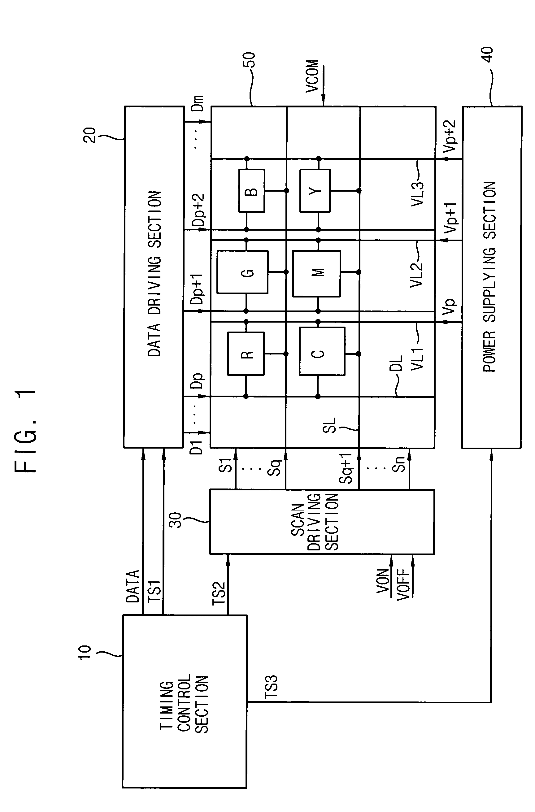
[0137]FIG. 19 is a schematic block diagram illustrating an OLED according to the invention. The OLED in FIG. 19 has a stripe-like sub pixel structure and each sub pixel may receive a different bias voltage.
[0138]Referring to FIG. 19, an OLED includes a timing control section 310, a data driving section 320, a scan driving section 330, a power supplying section 340, and an organic light emitting panel 350.
[0139]The timing control section 310 receives an image signal DATA and control signal thereof provided from an external graphic controller (not shown) to generate first, second and third timing signals TS1, TS2 and TS3. The timing control section 310 provides the data driving section 320 with the image signal DATA and the first timing signal TS1. The timing control section 310 provides the scan driving section 330 with the second timing signal TS2. The timing control section 310 provides the power supplying section 340 with the third timing signal TS3.
[0140]The data driving section ...
PUM
 Abstract
Description
Claims
Application Information