Assuring uniformity in the output of an OLED

a technology of uniformity and output, applied in the direction of instruments, static indicating devices, etc., can solve the problems of difficult accurate achievement, limited uniformity, and inability to accurately achieve the threshold voltage vth and the inclination of the v-i characteristics of respective pixels

Active Publication Date: 2010-12-28
GLOBAL OLED TECH
View PDF9 Cites 182 Cited by
  • Summary
  • Abstract
  • Description
  • Claims
  • Application Information

AI Technical Summary

Benefits of technology

[0012]In view of the problems described above, the present invention efficiently detects non-uniformity in an organic EL display device, calculates correction values, and performs correction.
[0018]Furthermore, according to the method of this invention, it is preferable that the two-dimensional space filter has coefficients of respective detection areas, so as to give a large weighting factor to the objective detection area, add a value of a peripheral detection area positioned closely to the objective detection area, and subtract a value of a peripheral detection area positioned far from the objective detection area.
[0019]Furthermore, with respect to the detection area that requires correction, it is possible to repeat the similar process on further divided areas to narrow the detection to a smaller detection area that requires correction. This reduces both the number of measurements and amount of time required.

Problems solved by technology

With such a configuration, there is a possibility that, the threshold voltage Vth and the inclination of the V-I characteristics of respective pixels may vary due to manufacturing errors.
However, with the former technique, it is generally difficult to accurately accomplish, within a short time, the measurement of the luminance for numerous pixels, while, with the latter technique, the correctable differences or nonuniformity is limited to the pixels having luminance values continuously changing along the entire display area or pixels having a specific pattern in the vertical or horizontal line.

Method used


Image

  • Assuring uniformity in the output of an OLED
  • Assuring uniformity in the output of an OLED
  • Assuring uniformity in the output of an OLED

Examples


Embodiment Construction

[0038]Hereinafter, a preferred embodiment of the present invention will be explained with reference to the attached drawings.

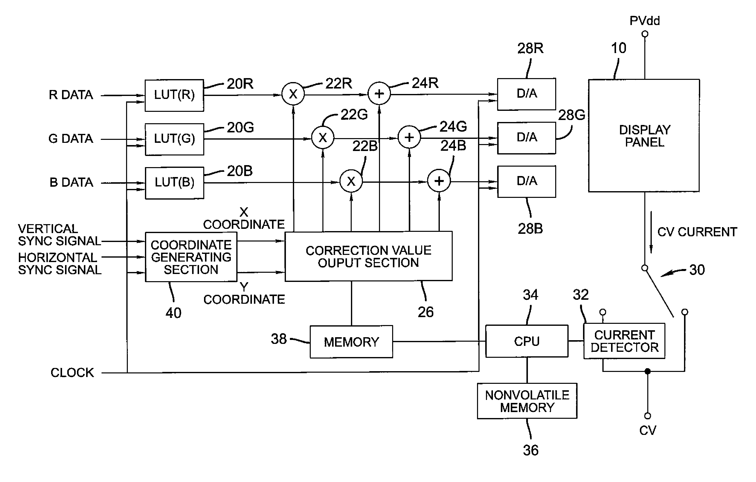
[0039]FIG. 4 shows the arrangement of an OLED display device in accordance with this embodiment, in which luminance data is input and corrected luminance data (i.e. analog signals) is output to be supplied to a display panel 10.

[0040]The display panel 10 has numerous pixels for respective RGB colors. The input data (i.e. pixel data, luminance data), being a voltage signal determining the luminance of each pixel, is input for each of respective RGB colors. For example, pixels of the same color are aligned in the vertical direction. One of RGB data signals is supplied to each data line to realize display of the color. According to this example, each of the RGB data is an 8-bit luminance data. The display panel 10 has the resolution of 320 pixels in the horizontal direction and 240 lines in the vertical direction. One pixel consists of three dots of RGB colors re...


PUM


Abstract

A display area of a display panel is divided into a plurality of areas, and a current detector detects a driving current (i.e. CV current) that flows when light is emitted from an area or a block including a plurality of areas. Such current detection is repeated while sequentially changing the target area or block and a CPU detects an area that has a current value different from that of other areas (i.e. an area that requires correction) based on results of the results of current detection. A similar process is performed on smaller areas obtained by subdividing the area to find a smaller area that requires correction. Thus, a correction value is obtained for each pixel and the correction values are efficiently calculated.

Description

FIELD OF THE INVENTION[0001]The present invention generally relates to a correction performed for assuring uniformity in the display of an organic EL display device that includes numerous organic EL elements arranged in a matrix pattern.BACKGROUND OF THE INVENTION[0002]Conventional organic EL (OLED) display devices including a plurality of organic EL (OLED) elements arranged in a matrix pattern are well known. Among these, attention is especially focused on active-matrix OLED display devices which are expected to become widely used in thin-type display devices. In active-matrix OLED display devices, transistors are provided for respective pixels to control a driving current supplied to each OLED element.[0003]FIG. 1 shows an example of a circuit arrangement for a pixel of a conventional active-matrix OLED display device. In this arrangement, a p-channel TFT (i.e. thin film transistor) 1, used for driving a pixel, has a source connected to a power source PVdd and a drain connected to...

Claims


Application Information

Patent Timeline
Patent Type & Authority Patents(United States)
IPC IPC(8): G09G3/30
CPCG09G3/3225G09G2320/0233G09G2320/0242G09G2320/0285G09G2320/029G09G2320/043
Inventor KOHNO, MAKOTO
Owner GLOBAL OLED TECH
Why Eureka
Try Eureka