Depository monitoring system in semiconductor storage warehouse

a monitoring system and semiconductor technology, applied in the direction of burglar alarm by hand-portable article removal, burglar alarm mechanical actuation, instruments, etc., can solve the problems of operator injury, wafer-based depository cannot be monitored in real time by the operator, and rfid techniques are not effectively integrated with the information system for depository monitoring

Inactive Publication Date: 2011-01-04
CHIPMOS TECH INC
View PDF7 Cites 1 Cited by
  • Summary
  • Abstract
  • Description
  • Claims
  • Application Information

AI Technical Summary

Benefits of technology

[0009]Therefore, a primary objective of the present invention is to provide a depository monitoring system integrated with RFID techniques, so that the operator or the system can monitor depository information of semiconductor objects using the RFID techniques in an on-line and real-time manner.
[0010]A second objective of the present invention is to provide a depository monitoring system integrated with RFID techniques, wherein an RFID tag can be coded as an index for searching, so that upstream and downstream manufactures can monitor present locations, conditions and test results of semiconductor objects in real time through an intranet.
[0013]A fifth objective of the present invention is to provide a depository monitoring system integrated with RFID techniques, whereby an operator in charge of goods receiving and shipping or assigned to an access control zone of a building can monitor inbound and outbound flows of semiconductor products in real time through an intranet.

Problems solved by technology

As a result, the wafer cassette 1010 may be mistakenly transported to a port by a mechanical arm, thereby injuring an operator.
While the prior art mentioned above uses RFID techniques to transport or track wafers, the RFID techniques are not effectively integrated with an information system for depository monitoring.
As a result, a wafer-based depository cannot be monitored in real time by the operator.
Therefore, it is a pressing issue in relevant industries to integrate RFID techniques into an information system for depository monitoring, so that the operator can perform on-line and real-time management of a depository of semiconductor products and a semiconductor testing schedule.

Method used


Image

  • Depository monitoring system in semiconductor storage warehouse
  • Depository monitoring system in semiconductor storage warehouse
  • Depository monitoring system in semiconductor storage warehouse

Examples


Embodiment Construction

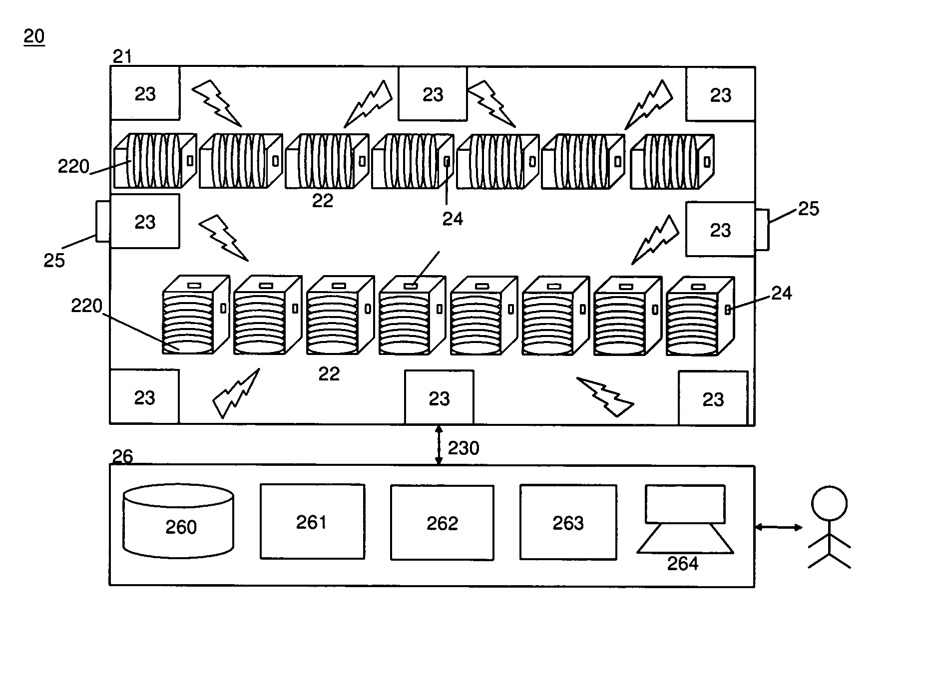
[0018]The present invention provides a depository monitoring system integrated with RFID techniques that allows an operator to conduct real-time wafer-based depository monitoring of carriers or semiconductor objects as well as production line management. Now that a person of ordinary skill in the art would readily understand the wafer testing procedure and the RFID theory involved in the present invention, a complete description thereof will not be given herein. Besides, drawings referred to in the following description are not drawn according to actual dimension and it is not necessary to do so because the drawings are intended to only schematically demonstrate structures related to features of the present invention.

[0019]Referring to FIG. 2 for a first preferred embodiment of the present invention, which is a depository monitoring system 20 integrated with RFID techniques for use in a semiconductor factory 21. The depository monitoring system 20 comprises a plurality of carriers 2...


PUM


Abstract

A depository monitoring system for use in a semiconductor factory comprises a plurality of carriers, each holding at least one semiconductor object; a depository monitoring host for monitoring a depository of each carrier; and a plurality of RFID tags and a plurality of RFID readers. It is characterized in that the RFID tags are disposed on the carriers and / or semiconductor objects, respectively, wherein each RFID tag has a tag information; the RFID readers read / write the tag information from / to the RFID tags; and the depository monitoring host comprises: a legacy database to store information related to the depository monitoring system; an RFID middleware for processing operations between the RFID readers and the RFID tags; a web interface for processing commands and query results through a B2B internet; an input / output interface for processing commands and query results through an intranet; and a depository controller for performing a sequence of processes in depository monitoring.

Description

BACKGROUND OF THE INVENTION[0001]1. Technical Field[0002]The present invention relates to a depository monitoring system and, more particularly, to a depository monitoring system integrated with radio frequency identification (RFID) techniques.[0003]2. Description of Related Art[0004]Prior art in relation to wafer inventory or transport using RFID techniques are disclosed in U.S. Pat. No. 6,330,971 (hereinafter referred to as '971), U.S. Patent Application Publication No. 20060043197 (hereinafter referred to as '197) and Taiwan Patent No. 1267029 (hereinafter referred to as '029). The '971 patent provides a wafer tracking system using RFID techniques, as shown in FIG. 1A, in which a system 10 comprises a plurality of wafer-carried carriers 11, an RFID reader 12, an RFID tag 14 mounted on each of the carriers 11, and a controller 13. The RFID reader 12 reads the RFID tag 14 mounted on each of the carriers 11 through a plurality of antennas 15 connected thereto, and then sends a tag i...

Claims


Application Information

Patent Timeline
Patent Type & Authority Patents(United States)
IPC IPC(8): G08B13/14
CPCG06Q10/08G06Q50/28
Inventor CHIANG, WEN-HSIANGFAN, TZU-CHUNGCHI, SHIH-TIHUANG, JUI-CHINGFAN, SHIENG CHIANGYI, CHI-MING
Owner CHIPMOS TECH INC
Why Eureka
Try Eureka