Shield flat cable and manufacturing method thereof

a flat cable and shield layer technology, applied in the direction of flat/ribbon cables, insulated conductors, cables, etc., can solve the problems of insufficient shield layer grounding, difficult to correctly position the holes with respect to the ground lines, and contact failure between the ground line and the shield layer

Active Publication Date: 2011-01-11
SUMITOMO ELECTRIC IND LTD
View PDF5 Cites 12 Cited by
  • Summary
  • Abstract
  • Description
  • Claims
  • Application Information

AI Technical Summary

Benefits of technology

[0008]Exemplary embodiments of the present invention provide a shield flat cable and a manufacturing method thereof in which a contact between ground lines and a shield layer is secured and a grounding of the shield layer is reliable.

Problems solved by technology

Therefore, when holes are formed through the insulating film on one side before the lamination, it is difficult to position the holes with respect to the ground lines correctly at a laminating position of a laminator because of positional errors of the running flat conductors, positional errors of the insulating film, positional errors of the holes in the running insulating film, and other factors.
The problem is particularly remarkable in the case where the adhesive layer of the insulating film is of a polyester type.
If incomplete holes are formed, a contact failure may occur between a ground line and the shield layer.
Thereby, the grounding of the shield layer becomes insufficient.
By the insufficient grounding of the shield layer insufficient, a phenomenon such that a noise is prone to be on a signal is caused, and a sufficient shield characteristic can not be obtained.
As a result, a contact failure probably occurs by obstruction of resin dregs.

Method used


Image

  • Shield flat cable and manufacturing method thereof
  • Shield flat cable and manufacturing method thereof
  • Shield flat cable and manufacturing method thereof

Examples


Embodiment Construction

[0030]An embodiment of a shield flat cable will be hereinafter described with reference to the drawings.

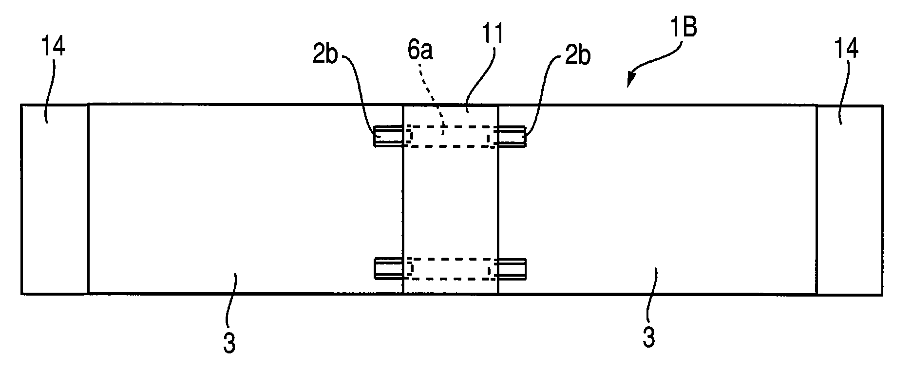
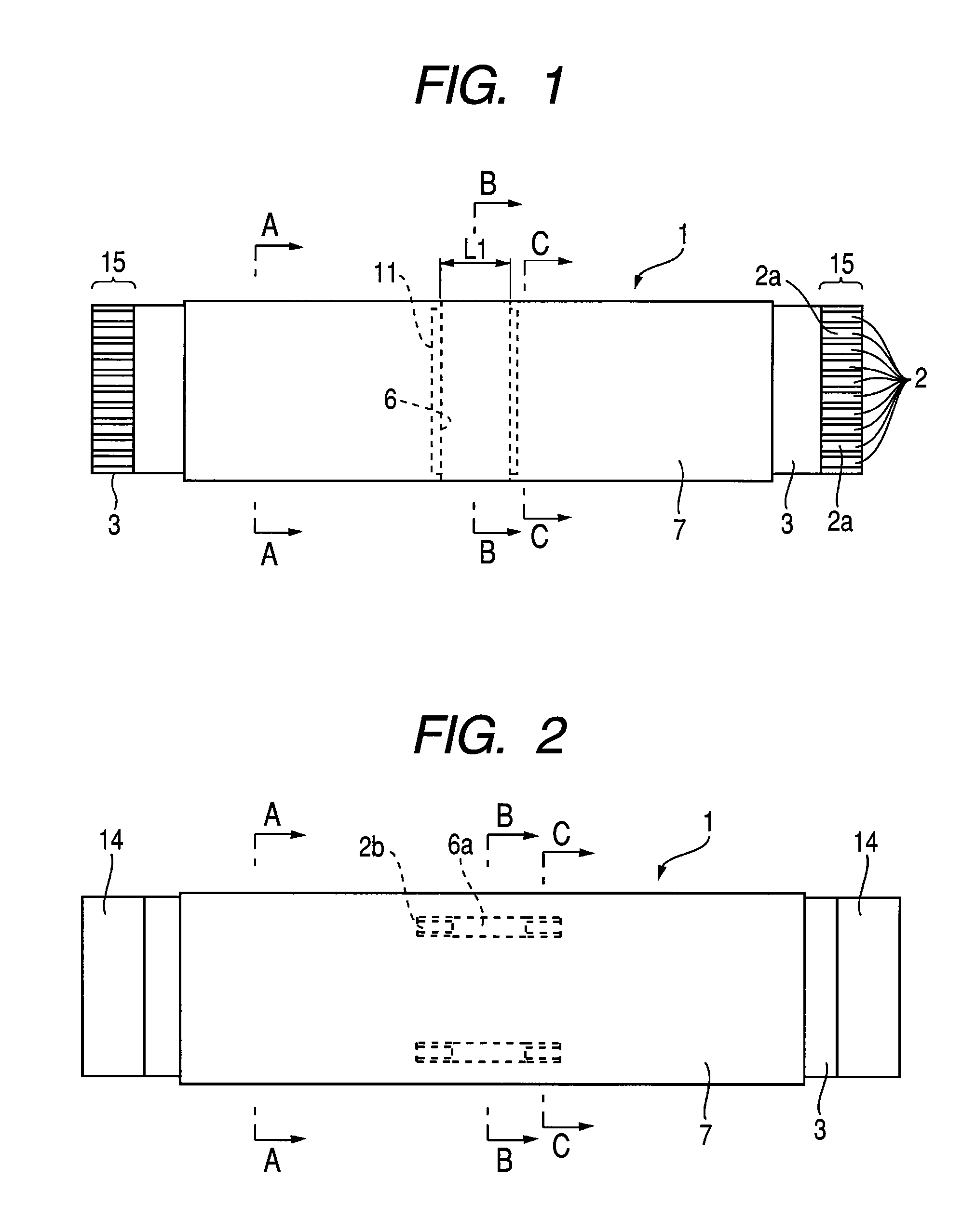
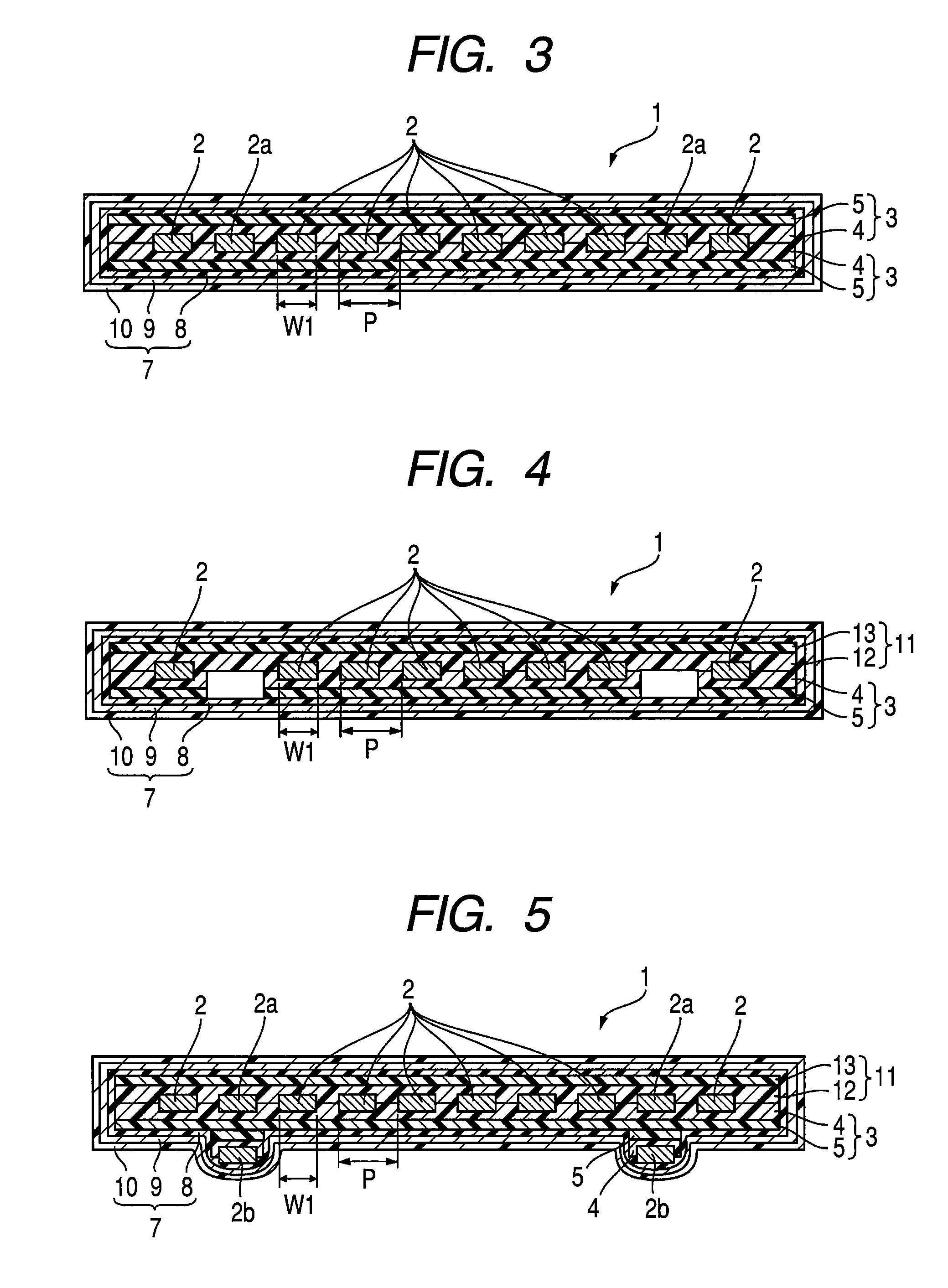
[0031]FIG. 1 is a plan view of one surface of the shield flat cable according to the embodiment. FIG. 2 is a plan view of the other surface of the shield flat cable of FIG. 1. FIG. 3 is a sectional view on arrow A-A in FIGS. 1 and 2. FIG. 4 is a sectional view on arrow B-B in FIGS. 1 and 2. FIG. 5 is a sectional view on arrow C-C in FIGS. 1 and 2. FIGS. 3 to 5 are drawn with the one surface of FIG. 1 as the top surface.

[0032]As shown in FIGS. 1 to 5, a shield flat cable 1 is provided with a plurality (in this embodiment, 10 strips) of flat conductors 2. The flat conductors 2 are arranged parallel with each other in one plane at a prescribed pitch. First insulating films 3 each including a first insulator are laminated on both surfaces of the flat conductors 2. A shield film 7 having a shield layer 9 is laminated on outside surfaces of the first insulating films 3. Both end portion...


PUM

PropertyMeasurementUnit
thicknessaaaaaaaaaa
thicknessaaaaaaaaaa
thicknessaaaaaaaaaa

Abstract

A manufacturing method of a flat shield cable has a step of arranging a plurality of flat conductors including a ground line parallel with each other in one plane at a pitch P, a step of forming a flat cable by laminating a first insulating film on the flat conductors from both sides of an arrangement plane of the flat conductors, a step of laminating a shield layer on outside surfaces of the flat cable, and a step of electrically connecting the ground line to the shield layer. The manufacturing method further has a step of cutting the ground line at a portion other than in the conductor exposure portions and folding cutting portions of the ground line to outside the first insulating film before laminating the shield layer, and a step of electrically connecting only the folded ground line among the flat conductors to the shield layer.

Description

FIELD OF THE INVENTION[0001]The present invention relates to a shield flat cable and a manufacturing method thereof which is used in electronic equipment or the like.DESCRIPTION OF RELATED ART[0002]Wiring members for electric wiring are now desired to enable high-density wiring in a limited space. Such wiring members include flexible circuit boards, flat cables using flat conductors, and electric connectors for connection of such circuit boards and cables. Shield flat cables having a shielding function are used for internal wiring of products requiring an anti-noise measure. For example, wiring of consumer equipment such as audio and video, OA equipment such as printers, scanners and copiers, DVD, CD-ROM, MO equipment, PCs and other electronic equipments.[0003]Flat cables are provided with a plurality of flat conductors arranged parallel with each other in one arrangement plane and insulating films laminated on the flat conductors from both sides of the arrangement plane. In the cas...

Claims


Application Information

Patent Timeline
Patent Type & Authority Patents(United States)
IPC IPC(8): H01B7/08
CPCH01B7/0861H01B7/0838Y10T29/49117
Inventor MATSUSHITA, KOYAMATSUDA, TATSUOYANAGIDA, KENKOBAYASHI, HIDEO
Owner SUMITOMO ELECTRIC IND LTD
Why Eureka
Try Eureka