Apparatus and methods for transporting and processing substrates

a technology of apparatus and substrates, applied in the direction of electrolysis components, vacuum evaporation coatings, coatings, etc., can solve the problems of increasing costs, increasing costs, and extremely high manufacturing costs of semiconductors, and achieves the effects of increasing costs, small footprint, and extremely high manufacturing costs

Active Publication Date: 2011-03-08
BOOKS AUTOMATION US LLC
View PDF4 Cites 41 Cited by
  • Summary
  • Abstract
  • Description
  • Claims
  • Application Information

AI Technical Summary

Benefits of technology

[0008]This invention is directed to a novel wafer processing unit intended to permit separately controlled dwell times at processing stations while maintaining a small footprint. It also allows ongoing operations even if one or more of the stations is down for one reason or another. In part this is in recognition that the costs of manufacturing semiconductors is extremely high and costs are increasing. The higher the costs the greater the risks in undertaking investments in this field. An objective is to define equipment that lowers costs by a reasonable percentage and provides improved systems and services in accordance with “Lean” principles of manufacture. Thus an objective is to maximize processing chambers while maintaining a small footprint. Another objective is to maximize process station utilization. Another objective is to simplify robotics and the service of this equipment. The system will also offer considerable redundancy, including up to 100% availability of the system for processing even during mainframe servicing. In such an event less chambers will be in use but all processes can continue to be available for treatment of wafers. And servicing or processing chambers will be possible from the back or front of the processing chambers. Additionally, in the preferred embodiment the processing chambers will be set up in a linear arrangement. This assures the smallest footprint for a system that permits individual programs for wafers at the various processing stations.
[0009]The processing chambers generally may have the capability of performing any of the various processes one uses in connection with processing wafers. For example in the manufacture of a wafer, the wafer would normally be carried through one or more etching steps, one or more sputtering or physical vapor deposition processes, ion implantation, chemical vapor deposition (CVD) and heating and / or cooling processes, among others. The number of processing steps to make a wafer could mean that multiple tools or tools with large subsystems would have been required if using prior art devices to perform these various processes. The instant system however, offers the further advantage that additional functional stations can be added without a significant increase in size or without the need to add new total systems.

Problems solved by technology

In part this is in recognition that the costs of manufacturing semiconductors is extremely high and costs are increasing.
The higher the costs the greater the risks in undertaking investments in this field.
The system will also offer considerable redundancy, including up to 100% availability of the system for processing even during mainframe servicing.

Method used


Image

  • Apparatus and methods for transporting and processing substrates
  • Apparatus and methods for transporting and processing substrates
  • Apparatus and methods for transporting and processing substrates

Examples


Embodiment Construction

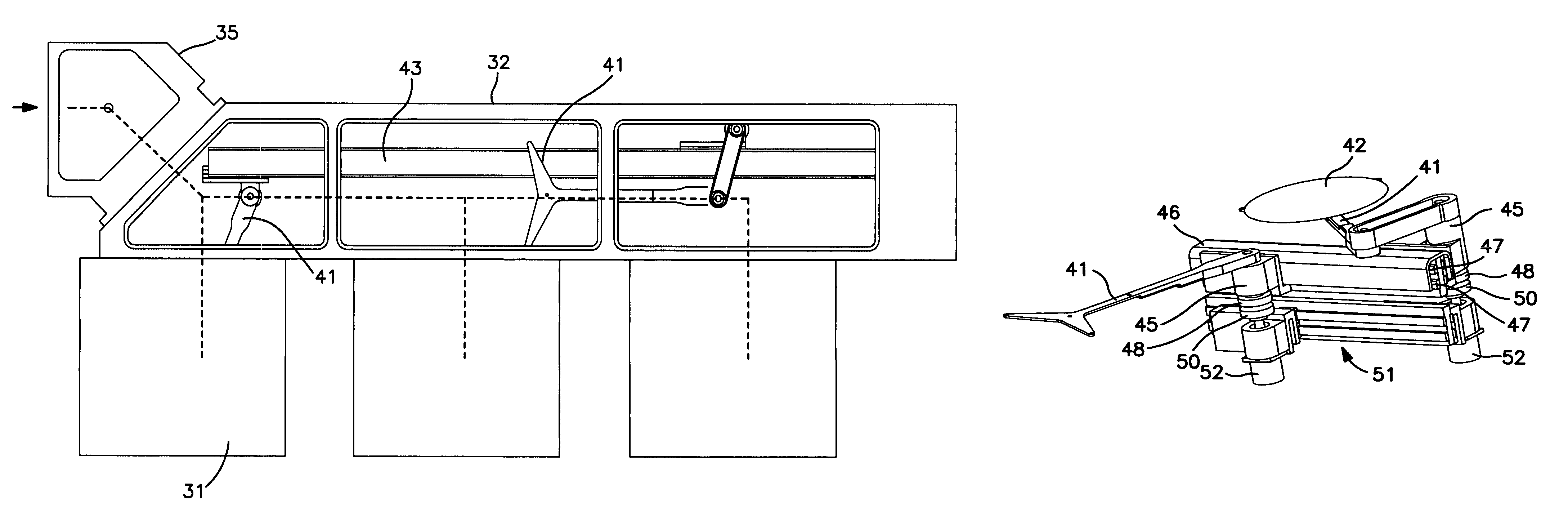
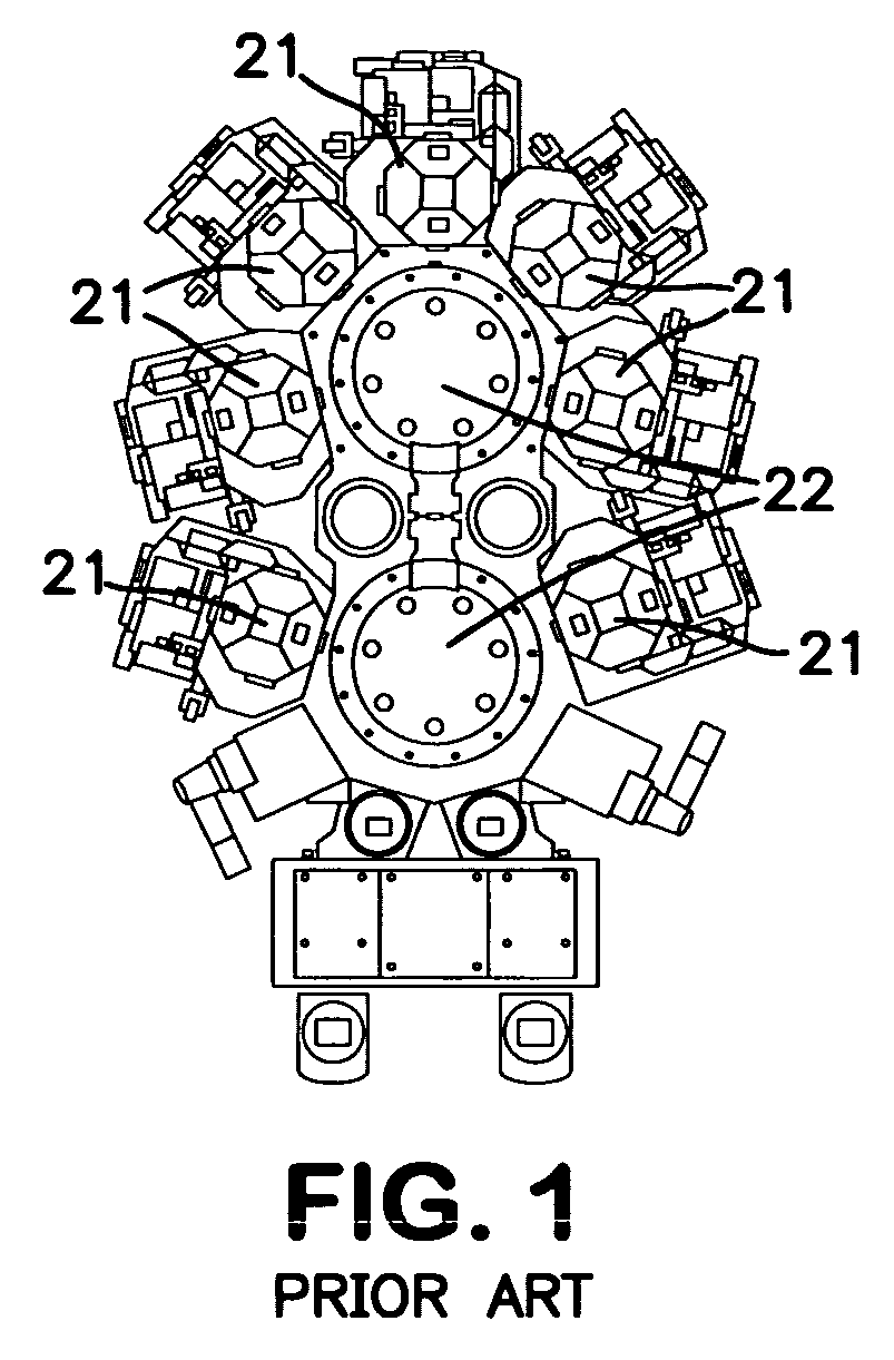
[0023]Referring now to FIG. 1, there is illustrated a cluster tool of the type commonly in use today. In general this comprises processing chambers 21 radially disposed around and attached to central chambers 22. In this system, there are two central chambers. Other systems may have only a single central chamber. A system with more than two can exist except that it is cumbersome and instead users will generally acquire another system. In operation, a robot is typically located within each central chamber 22. The robot receives wafers into the system and carries wafers from the central chamber to processing chambers and after processing back to the central chamber. In some prior art systems, a central robot can access only a single wafer and single chamber at one time. Thus the robot can become engaged or busy during processing in connection while a wafer is in a single chamber. This combination of a single robot tied to a processing station during processing is a limitation on the t...


PUM

PropertyMeasurementUnit
diameteraaaaaaaaaa
diameteraaaaaaaaaa
diameteraaaaaaaaaa

Abstract

There is described apparatus and methods for transporting and processing substrates including wafers as to efficiently produce at reasonable costs improved throughput as compared to systems in use today. A key element is the use of a transport chamber along the sides of processing chambers for feeding substrates into a controlled atmosphere through a load lock and then along a transport chamber as a way of reaching processing chambers and then out of the controlled atmosphere following processing in the processing chambers.

Description

FIELD OF THE INVENTION[0001]This invention has to do with novel apparatus and methods for transporting and processing substrates in general and wafers in particular.BACKGROUND[0002]In the manufacture of semiconductors, a common tool, referred to as a cluster tool, is one of the key units used in the manufacture of wafers. A typical commercial device has a generally circular central area with chambers attached along the circumference. The chambers extend outward around the central area. When wafers are processed they are moved first from an input output station on the circumference of the central chamber into the central chamber and then from the central chamber into an attached or circumferential chamber where processing is performed. In this tool as in substantially all manufacturing systems used today, the practice is to process wafers one at a time. A wafer may be moved into a chamber for processing and then back to the central chamber. This can be followed by a further move to a...

Claims


Application Information

Patent Timeline
Patent Type & Authority Patents(United States)
IPC IPC(8): C23F1/00C23C14/00H01L21/306C23C16/00
CPCH01L21/67173H01L21/67184H01L21/67745H01L21/67201H01L21/67196
Inventor BLUCK, TERRYFAIRBAIRN, KEVIN PBARNES, MICHAEL S.LANE, CHRISTOPHER T.
Owner BOOKS AUTOMATION US LLC
Why Eureka
Try Eureka