Semiconductor device having super junction structure

a technology of super junction and semiconductors, applied in the direction of semiconductor devices, basic electric elements, electrical appliances, etc., can solve the problems of high breakdown voltage and low resistance, increase of leak current in the pn column layer b>30/b>, and increase the number of voids generated in the pn column layer. , the effect of reducing the number of voids

Inactive Publication Date: 2011-03-29
DENSO CORP
View PDF15 Cites 0 Cited by
  • Summary
  • Abstract
  • Description
  • Claims
  • Application Information

AI Technical Summary

Benefits of technology

When the PN column layer is formed, a plurality of trenches is formed in the semiconductor substrate and the trenches are filled by an epitaxial growth, for example. In the present semiconductor device, the number of void that is generated in the PN column layer when the PN column layer is formed by the above-described method can be reduced. Thus, a breakdown voltage can be improved and a leak current can be reduced.
In the above-described manufacturing method, the number of void generated in the PN column layer can be reduced. Thus, in the semiconductor device manufactured by the above-described method, a breakdown voltage can be improved and a leak current can be reduced.

Problems solved by technology

However, in the vertical MOS transistor, a high breakdown voltage and a low on resistance have a trade-off relationship therebetween.
However, when the p type columns 2p are formed, a void may be generated in the PN column layer 30 depending on a condition, and thereby the high breakdown voltage may not be obtained and the leak current in the PN column layer 30 may increase.

Method used


Image

  • Semiconductor device having super junction structure
  • Semiconductor device having super junction structure
  • Semiconductor device having super junction structure

Examples


Embodiment Construction

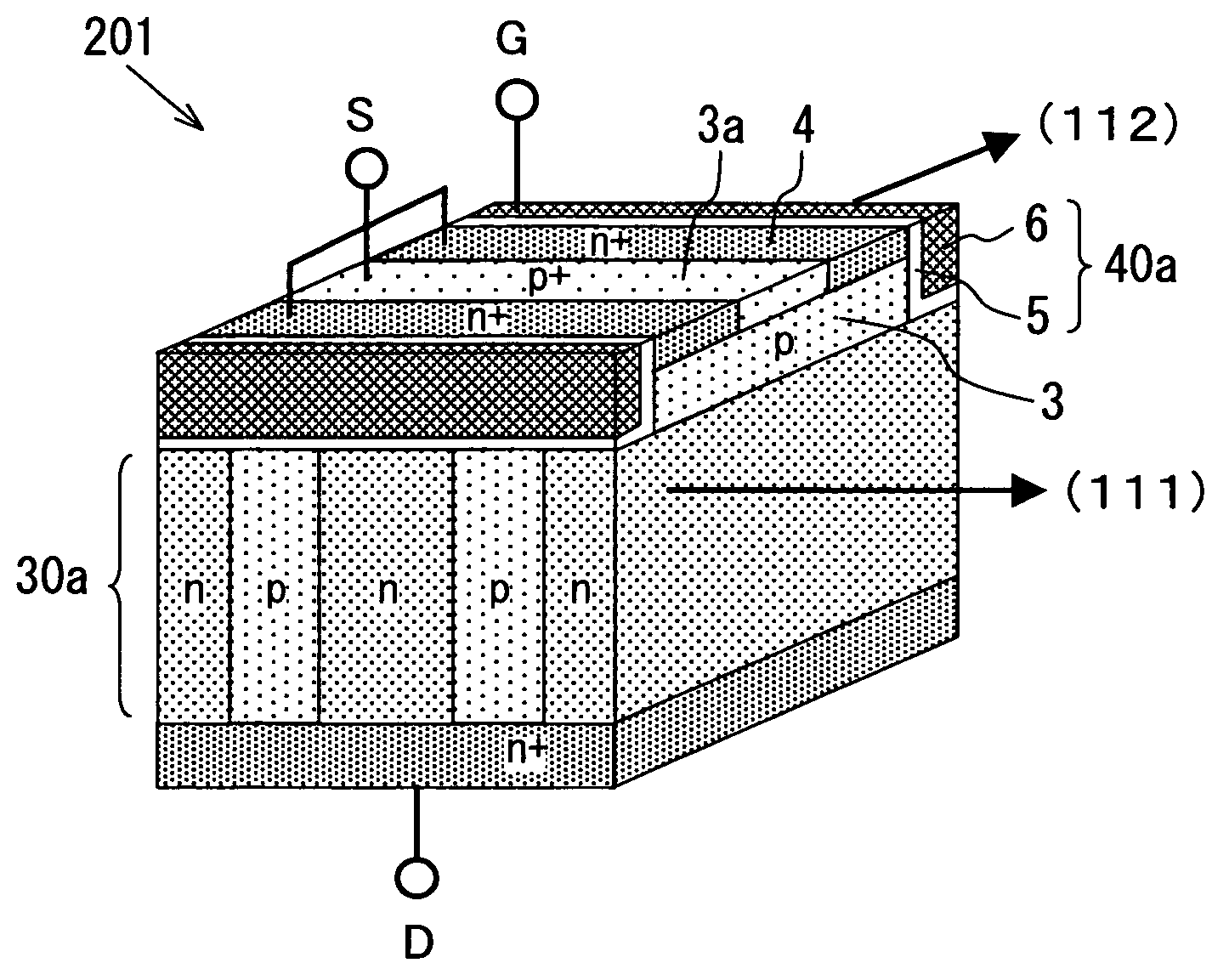
A super-junction metal oxide semiconductor (SJ-MOS) 201 according to a first example of an embodiment of the invention will now be described with reference to FIGS. 1A and 1B. The SJ-MOS 201 is an N-channel SJ-MOS and has an N+ type silicon substrate 1a functioning as a drain region. The SJ-MOS 201 has a PN column layer 30a on the silicon substrate 1a. The PN column layer 30a is an epitaxial layer made of silicon and includes N type columns 2n and P type columns 2p. The N type columns 2n and the P type columns 2p have approximately rectangular parallelepiped shapes and are alternately arranged on the silicon substrate 1a.

On the PN column layer 30a, a P type layer 3 functioning as a channel-forming layer is formed. For example, the P type layer 3 is obtained by an epitaxial layer made of silicon or ion implantation. At surface portions of the P type layer 3, N+ type regions 4 functioning as source regions are formed. Trench insulation gate electrodes (gate electrodes) 40a are dispos...


PUM


Abstract

A semiconductor device includes a silicon substrate having a (110)-oriented surface, a PN column layer disposed on the (110)-oriented surface, a channel-forming layer disposed on the PN column layer, a plurality of source regions disposed at a surface portion of the channel-forming layer, and gate electrodes penetrate through the channel-forming layer. The PN column layer includes first columns having a first conductivity type and second columns having a second conductivity type which are alternately arranged in such a manner that the first columns contact the second columns on (111)-oriented surfaces, respectively. The gate electrodes are adjacent to the source regions, respectively, and each of the gate electrodes has side surfaces that cross the contact surfaces of the first columns and the second columns in a plane of the silicon substrate.

Description

CROSS REFERENCE TO RELATED APPLICATIONThe present application is based on and claims priority to Japanese Patent Application No. 2007-128565 filed on May 14, 2007, the contents of which are incorporated in their entirety herein by reference.BACKGROUND OF THE INVENTION1. Field of the InventionThe present invention relates to a semiconductor device having a super junction structure and method of manufacturing the same.2. Description of the Related ArtConventionally, a vertical metal-oxide-semiconductor (MOS) transistor can be highly integrated compared with a horizontal MOS transistor. Thus, the vertical MOS transistor can be suitably used for an electrical application, for example, for controlling electric power. However, in the vertical MOS transistor, a high breakdown voltage and a low on resistance have a trade-off relationship therebetween.A semiconductor device that has a PN column layer functioning as a super junction (SJ) as a drift layer, that is, an SJ-MOS can improve a trad...

Claims


Application Information

Patent Timeline
Patent Type & Authority Patents(United States)
IPC IPC(8): H01L29/78
CPCH01L29/0634H01L29/66734H01L29/7813H01L29/045H01L29/0696H01L29/1045
Inventor SHIBATA, TAKUMIYAMAUCHI, SHOUICHI
Owner DENSO CORP
Why Eureka
Try Eureka