Solid state light sheet and encapsulated bare die semiconductor circuits with electrical insulator

a semiconductor circuit and solid-state light sheet technology, applied in the direction of optics, radio frequency control devices, instruments, etc., can solve the problems of high the requirement of a high-intensity photo-radiation source, and the cost of forming the lamp and then soldering the lamp to the printed circuit board is a relatively expensive process, and achieves a high density of die packing.

Inactive Publication Date: 2011-05-31
ARTICULATED TECH LLC
View PDF11 Cites 93 Cited by
  • Summary
  • Abstract
  • Description
  • Claims
  • Application Information

AI Technical Summary

Benefits of technology

[0043]A light emitting device includes a first bottom substrate having an electrically conductive surface. A second bottom substrate having an electrically conductive surface is provided adjacent to but electrically isolated from the first bottom substrate. A first bare die light emitting diode device having a top p junction conductor and a bottom n junction conductor is provided in electrical communication with the electrically conductive surface of the first bottom conductor. A second bare die light emitting diode device having a top n junction conductor and a bottom p junction conductor is provided in electrical communication with the electrically conductive surface of the second bottom conductor. The p / n junctions of the diodes may be reversed. A top substrate has a conductive surface in electrical communication with both the top p junction conductor of the first bare die light emitting diode device and the top n junction conductor of the second bare die light emitting diode device. The electrically conductive surface of the top substrate is effective for putting the first bare die light emitting diode device and the second bare die light emitting diode device into a series electrical connection.
[0118]In accordance with another aspect of the present invention, the photo-radiation source includes a first electrode with a second electrode disposed adjacent to the first electrode, and defining a gap therebetween. A photo-radiation emission layer is disposed in the gap. The photo-radiation emission layer includes a charge-transport matrix material and an emissive particulate dispersed within the charge-transport matrix material. The emissive particulate receives electrical energy through the charge-transport matrix material applied as a voltage to the first electrode and the second electrode photo-radiation. The emissive particulate generates photo-radiation in response to the applied voltage. This photo-radiation is effective for the selective polymerization of photo-radiation curable organic material.

Problems solved by technology

The conversion of an LED die into an LED lamp is a costly process, involving very precise handling and placement of the tiny LED die.
The cost of forming the lamp and then soldering the lamp to a printed circuit board is a relatively expensive process.
Among the drawbacks of the conventional systems that utilize photo-polymerizable organic materials is the requirement of a high intensity photo-radiation source.
However, these light sources are an inefficient radiation source because most of the energy put in to drive the lamp is wasted as heat.
This heat must be removed from the system, increasing the overall bulk and cost.
Also, the lamps have relatively short service life-times, typically around 1000 hours, and are very costly to replace.
Much of the light output is wasted.
This UV radiation is harmful to humans, and additional shielding and protective precautions such as UV-filtering goggles are needed to protect the operators of such equipment.
It is very difficult to manufacture these conventional lamps due to the very small size of the die, and the need to solder or wire bond such a small wire to such a small die electrode.
Further, the plastic lens material is a poor heat conductor and the cup provides little heat sink capacity.
As the die heats up its efficiency is reduced, limiting the service conditions, power efficiency and light output potential of the lamp.
The bulkiness of the plastic lens material and the need to solder or wire bond the lamp leads to an electrical power source limits emissive source packing density and the potential output intensity per surface area.
However, the processing that takes the LED dice and turns it into an LED lamp is tedious and sophisticated, mostly due to the very small size of the LED die.
It is very difficult to solder or wire bond directly to the dice, and so it is common practice to use LED lamps that are then solder or wire bonded onto a circuit board.
This solution is far from optimum, since the relatively high cost of the LED lamps keeps the overall cost of the photo-radiation source high.
But, replacing the conventionally-used opaque wire with a transparent electrode film is not new and is in the public domain (see, Lawrence et al, U.S. Pat. No. 4,495,514).

Method used


Image

  • Solid state light sheet and encapsulated bare die semiconductor circuits with electrical insulator
  • Solid state light sheet and encapsulated bare die semiconductor circuits with electrical insulator
  • Solid state light sheet and encapsulated bare die semiconductor circuits with electrical insulator

Examples


Embodiment Construction

[0384]For purposes of promoting an understanding of the principles of the invention, reference will now be made to the embodiments illustrated in the drawings and specific language will be used to describe the same. It will nevertheless be understood that no limitation of the scope of the invention is thereby intended, there being contemplated such alterations and modifications of the illustrated device, and such further applications of the principles of the invention as disclosed herein, as would normally occur to one skilled in the art to which the invention pertains.

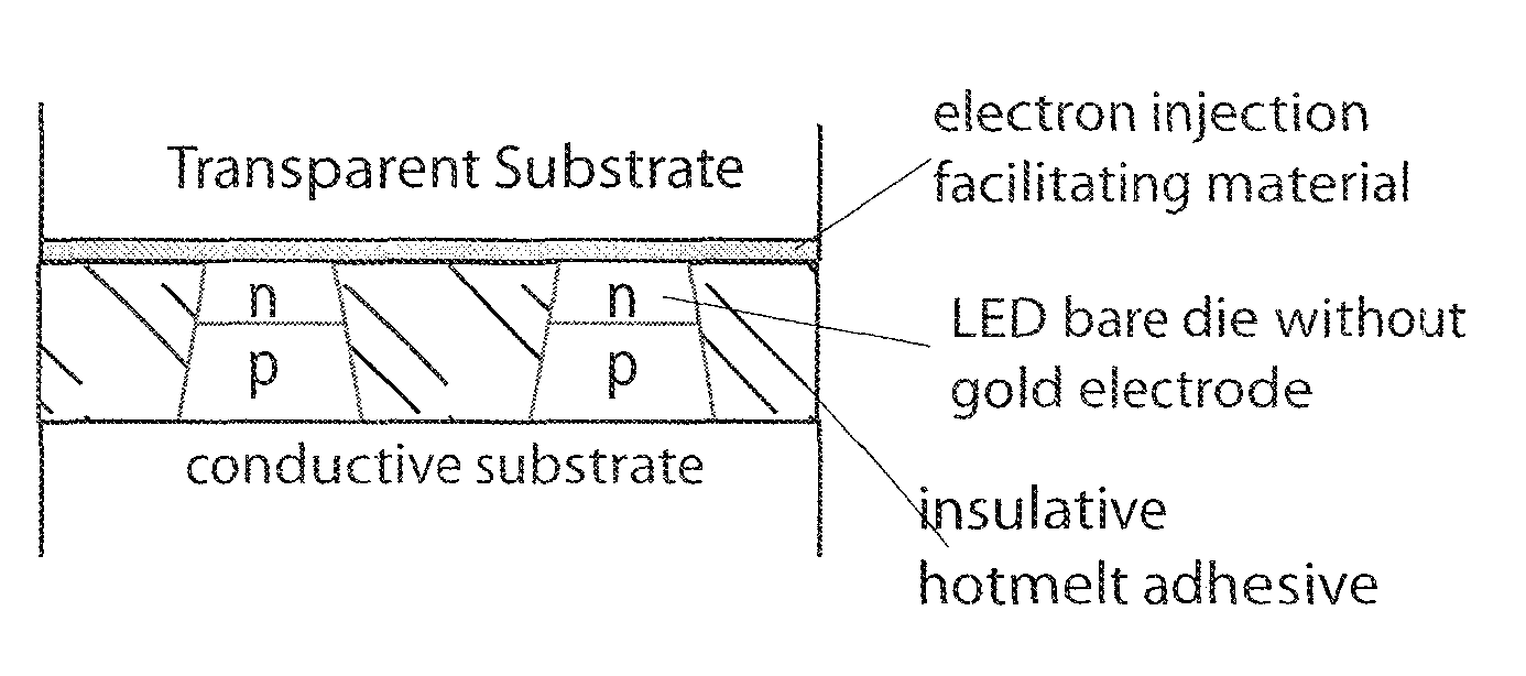
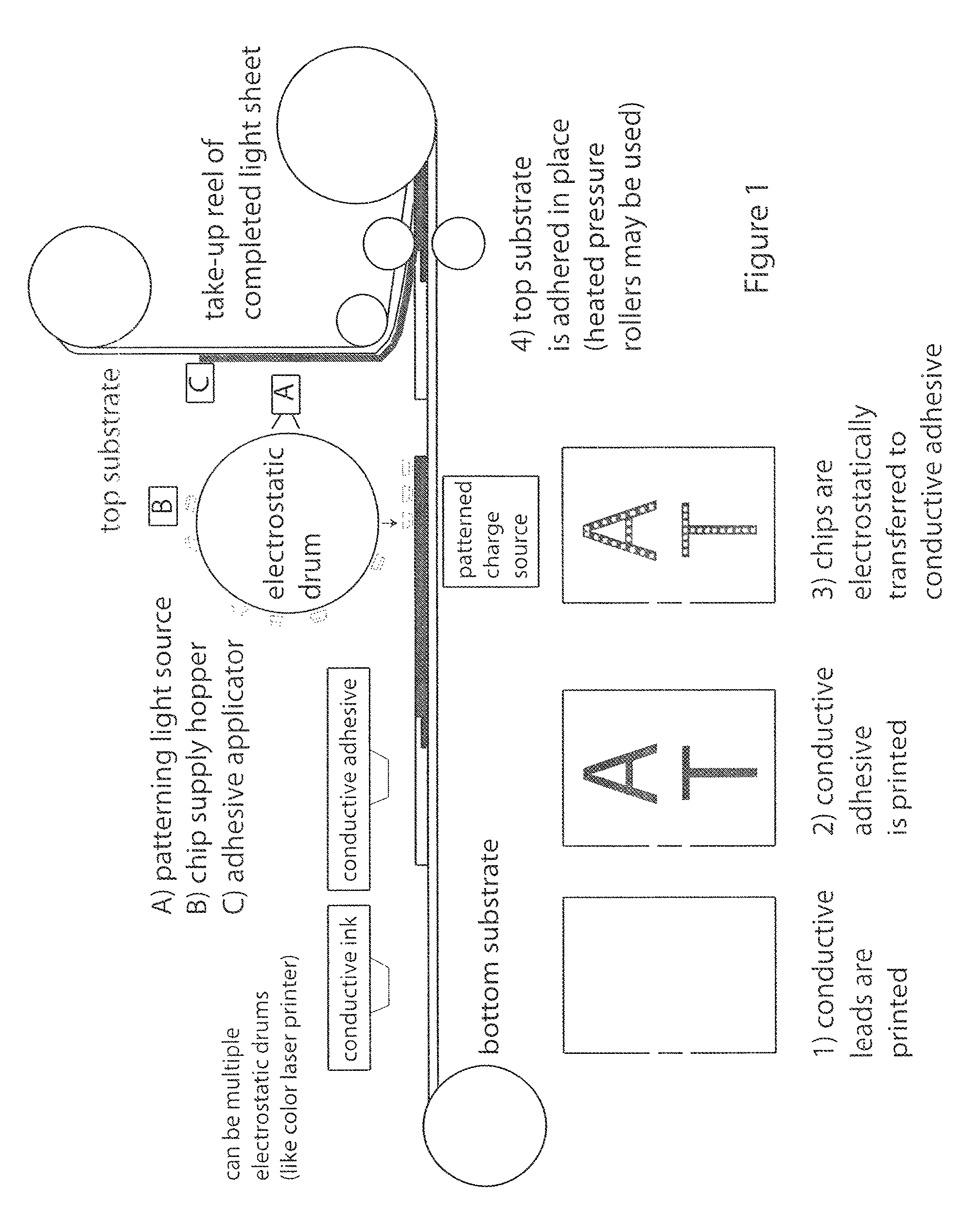
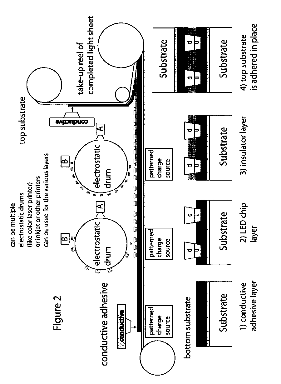
[0385]FIG. 1 illustrates the inventive method for manufacturing a patterned light active sheet. In accordance with the present invention, a solid-state light active sheet, and a method for manufacturing the same, is provided. The solid-state light active sheet is effective for applications such as flexible solar panels and light sensors, as well as high efficiency lighting and display products. The inventive light she...


PUM


Abstract

An electronically active sheet includes a bottom substrate having a bottom electrically conductive surface. A top substrate having a top electrically conductive surface is disposed facing the bottom electrically conductive surface. An electrical insulator separates the bottom electrically conductive surface from the top electrically conductive surface. At least one bare die electronic element is provided having a top conductive side and a bottom conductive side. Each bare die electronic element is disposed so that the top conductive side is in electrical communication with the top electrically conductive surface and so that the bottom conductive side is in electrical communication with the bottom electrically conductive surface.

Description

CROSS-REFERENCE TO RELATED APPLICATIONS[0001]This application is a continuation application of U.S. Utility application Ser. No. 11 / 585,724, entitled Solid State Light Sheet and Encapsulated Bare Die Semiconductor Circuits, filed Oct. 24, 2006, which is a continuation-in-part application of U.S. Utility application Ser. No. 11 / 454,479, entitled Solid State Light Sheet and Bare Die Semiconductor Circuits with Series Connected Bare Die Circuit Elements, which is a continuation-in-part application of U.S. Utility application Ser. No. 11 / 029,129, entitled Roll-to-Roll Fabricated Light Sheet and Encapsulated Semiconductor Circuit Devices filed Jan. 4, 2004, and U.S. Utility application Ser. No. 11 / 029,137, entitled Roll-to-Roll Fabricated Light Sheet and Encapsulated Semiconductor Circuit Devices filed Jan. 4, 2004, both of which are continuation-in-part applications of U.S. Utility application Ser. No. 10 / 919,830, entitled Light Active Sheet And Methods For Making The Same, filed Aug. 1...

Claims


Application Information

Patent Timeline
Patent Type & Authority Patents(United States)
IPC IPC(8): H01L27/15H01L31/00H01L31/12H01L33/52H01L33/56
CPCH01L24/75G02F1/133603H01L33/52H01L33/56H01L2924/07802H01L2924/12041H01L2924/00H01L2924/12044
Inventor DANIELS, JOHN JAMESNELSON, GREGORY VICTOR
Owner ARTICULATED TECH LLC
Why Eureka
Try Eureka