

Electro-optical device, driving circuit and driving method of the same, and electronic apparatus
a technology of optical devices and electronic devices, applied in the direction of electric digital data processing, instruments, computing, etc., can solve the problems of inability to perform appropriate gray scale display, affecting the response speed of display elements, and limited number of addressable luminance levels that can be displayed, so as to increase the number of addressable luminance levels.
- Summary
- Abstract
- Description
- Claims
- Application Information
AI Technical Summary
Benefits of technology
Problems solved by technology
Method used
Image

Examples
first embodiment
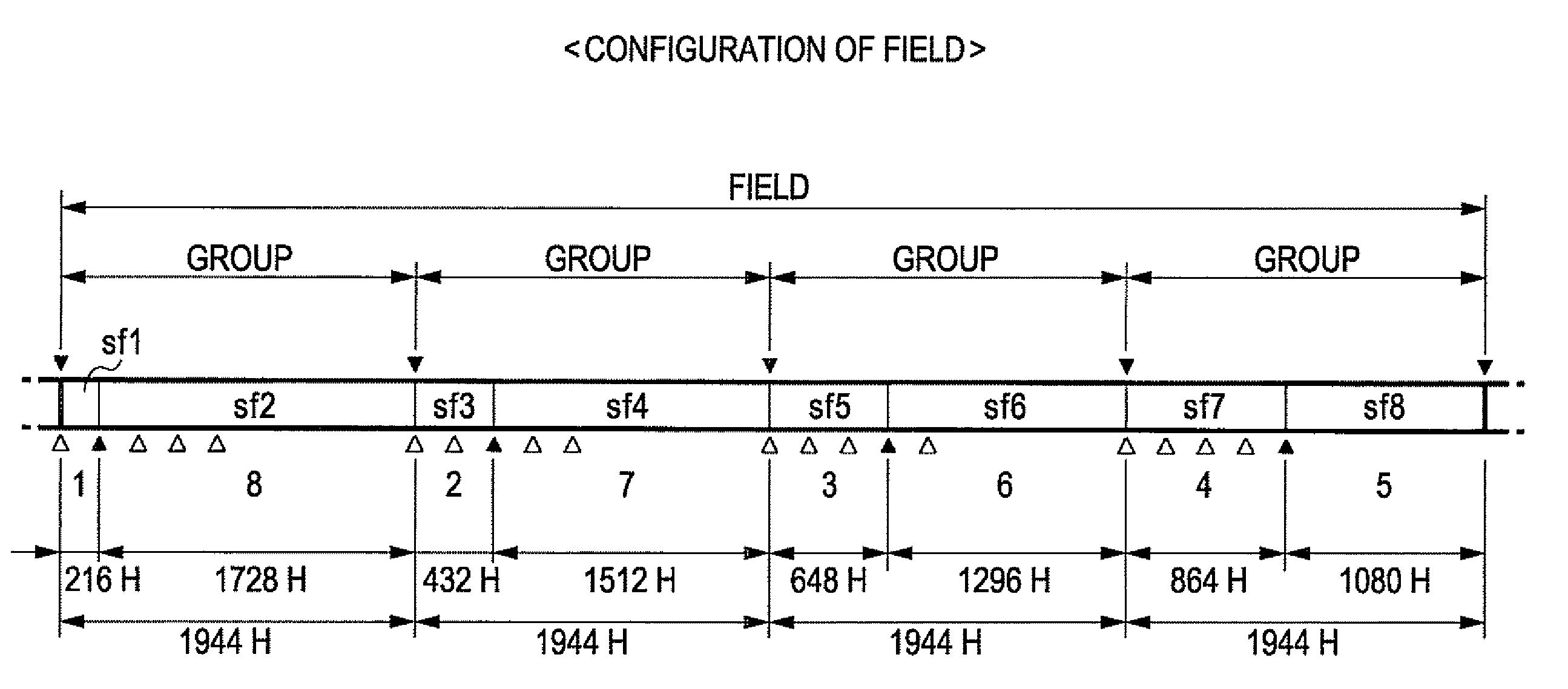
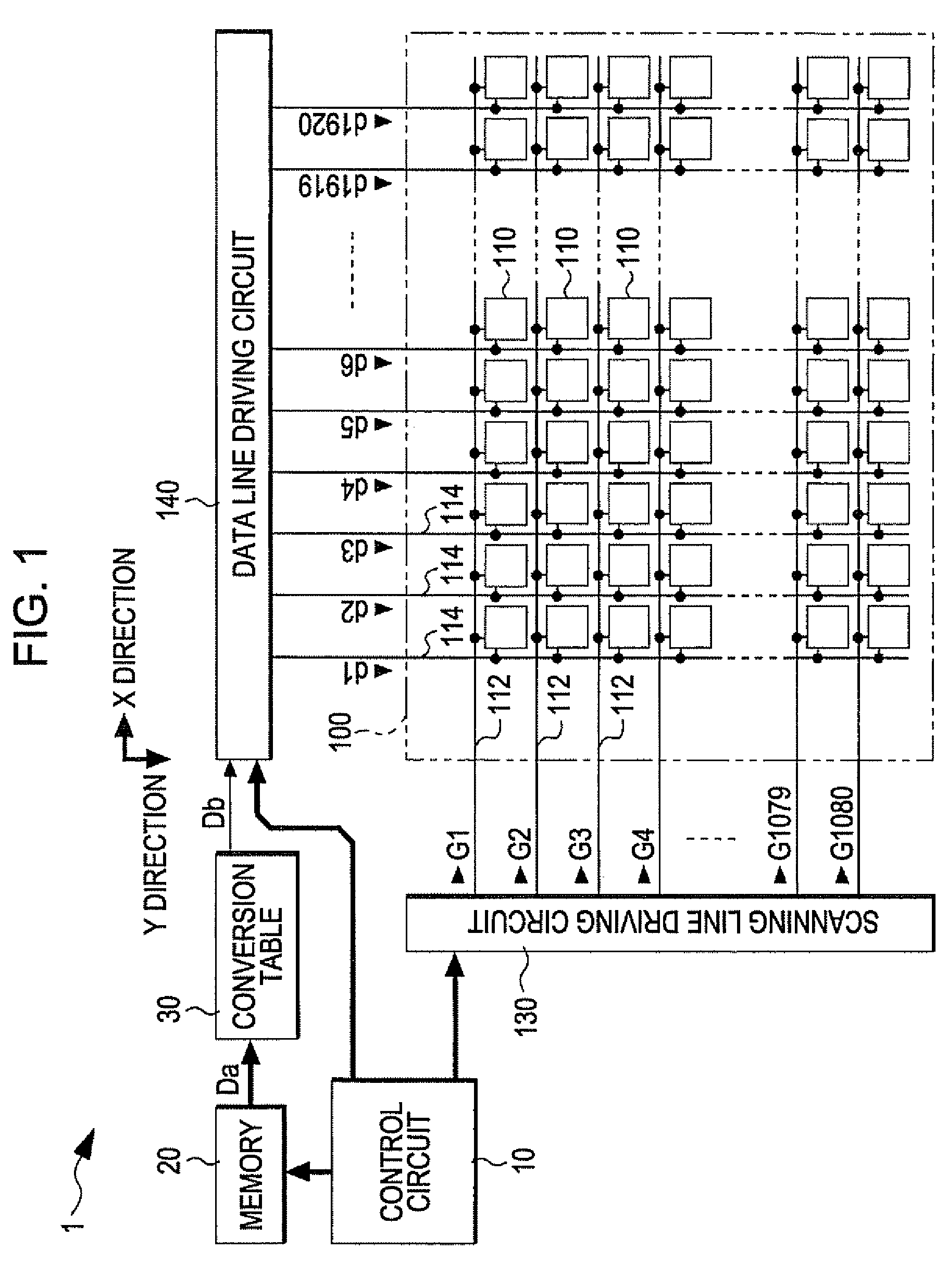
[0037]First, a first embodiment of the invention will be described. FIG. 1 is a block diagram that shows the overall configuration of an electro-optical device 1 according to the first embodiment. As shown in the drawing, the electro-optical device 1 roughly includes a control circuit 10, a memory 20, a conversion table 30, a display circuit 100, a scanning line driving circuit 130 and a data line driving circuit 140. The control circuit 10 controls portions of the electro-optical device 1, as will be described later. The display circuit 100 includes pixels that are arranged in a matrix. Specifically, the display circuit 100 includes 1080 scanning lines 112 that extend in an X (horizontal) direction in the drawing and 1920 data lines 114 that are electrically insulated from the scanning lines 112 and that extend in a Y (vertical) direction in the drawing. Then, the pixels 110 are provided at portions corresponding to intersections of the scanning lines 112 and the data lines 114. Th...
second embodiment
[0090]In the first embodiment, the liquid crystal elements 120 are made to enter any one of an on state or an off state over the sub-fields sf1 to sf8; however, multiple gray scales may be achieved by adding an intermediate (half) voltage in addition to these on state and off state without changing the configuration of the sub-fields. FIG. 17 is a view that shows allocation of an on state, a half state, or an off state to the sub-fields sf1 to sf8 in regard to gray-scale levels in steps of one level from “0.5” to “35.5”. When each of the liquid crystal elements 120 is set to a normally black mode, each liquid crystal element 120 tends to appear white color corresponding to an on state when the pixel electrode 118 is applied with the voltage Vw(+) or Vw(−) and tends to appear black color corresponding to an off state when the pixel electrode 118 is applied with the voltage Vb(+) or Vb(−). Thus, when a voltage Vg(+), which is the intermediate voltage between the voltages Vw(+) and Vb(...
PUM
 Abstract
Description
Claims
Application Information