Semiconductor device including a resurf region with forward tapered teeth

a technology of resurf region and resurf region, which is applied in the direction of semiconductor devices, basic electric elements, electrical appliances, etc., and can solve problems such as reliability reduction

Active Publication Date: 2011-08-02
KK TOSHIBA
View PDF16 Cites 11 Cited by
  • Summary
  • Abstract
  • Description
  • Claims
  • Application Information

AI Technical Summary

Problems solved by technology

The electric field concentration may contribute to the reliability reduction, including the leak current variation, and the device breakdown due to the breakdown voltage reduction in the terminal region.

Method used


Image

  • Semiconductor device including a resurf region with forward tapered teeth
  • Semiconductor device including a resurf region with forward tapered teeth
  • Semiconductor device including a resurf region with forward tapered teeth

Examples


first embodiment

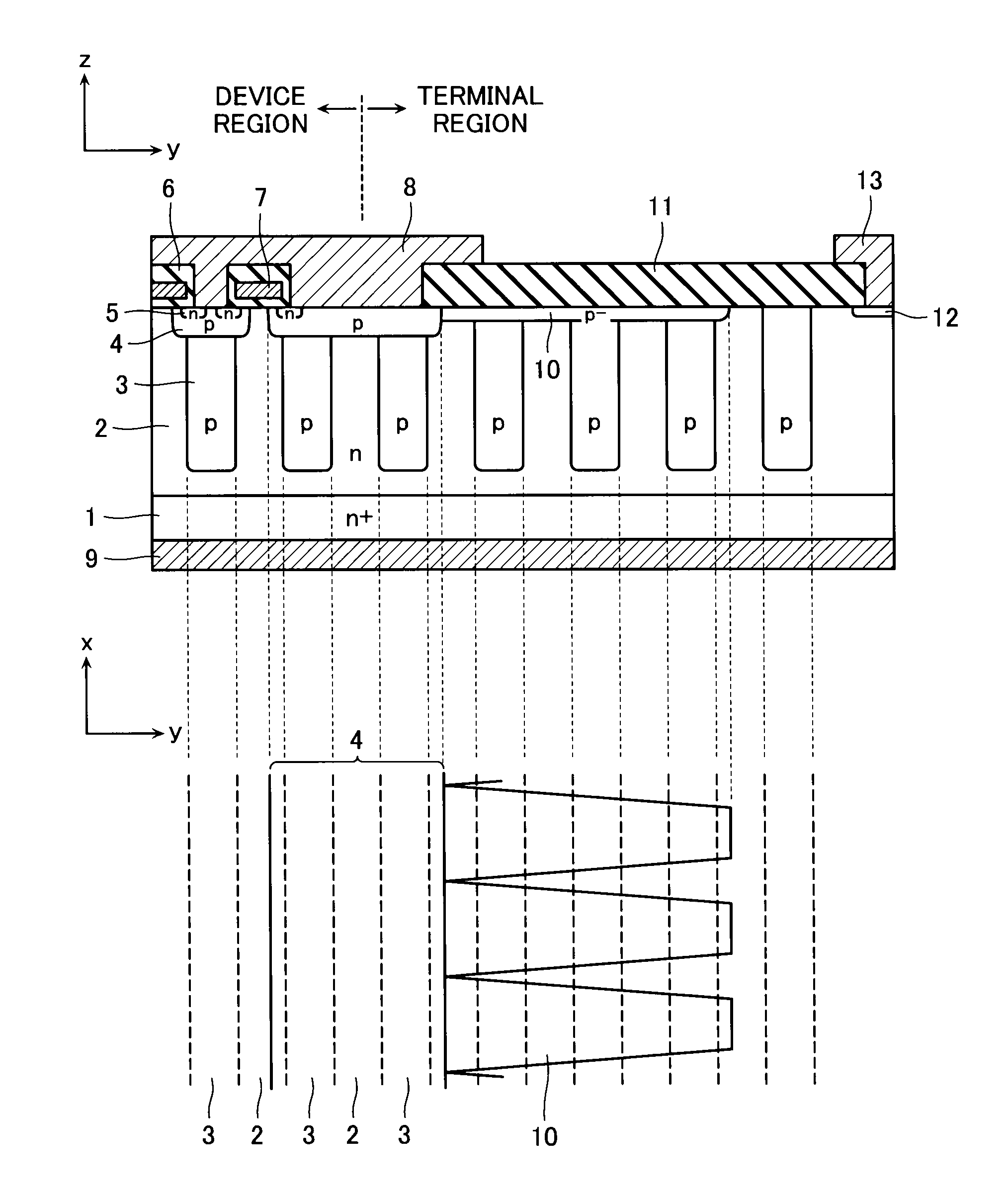
[0032]FIG. 1 is a cross-sectional view and a plan view of the structure of a semiconductor device according to a first embodiment of the present invention. In FIG. 1, the upper portion is a cross-sectional view of the semiconductor device taken along the y-z plane. The lower portion in FIG. 1 is a plan view taken along the x-y plane. In FIG. 1, the semiconductor device of this embodiment is an n channel planar-gate type MOSFET having a super junction region to which the present invention is applied. FIG. 1 shows a device region and a terminal region of the MOSFET.

[0033]With reference to FIG. 1, the semiconductor device in this embodiment is formed on an n+ type semiconductor substrate 1. The substrate 1 has top and bottom surfaces that are opposed to each other. The substrate 1 is made of, for example, silicon (Si). On the top surface of the n+ type semiconductor substrate 1, the device region and the terminal region are formed. Both of the device and terminal regions include an n t...

second embodiment

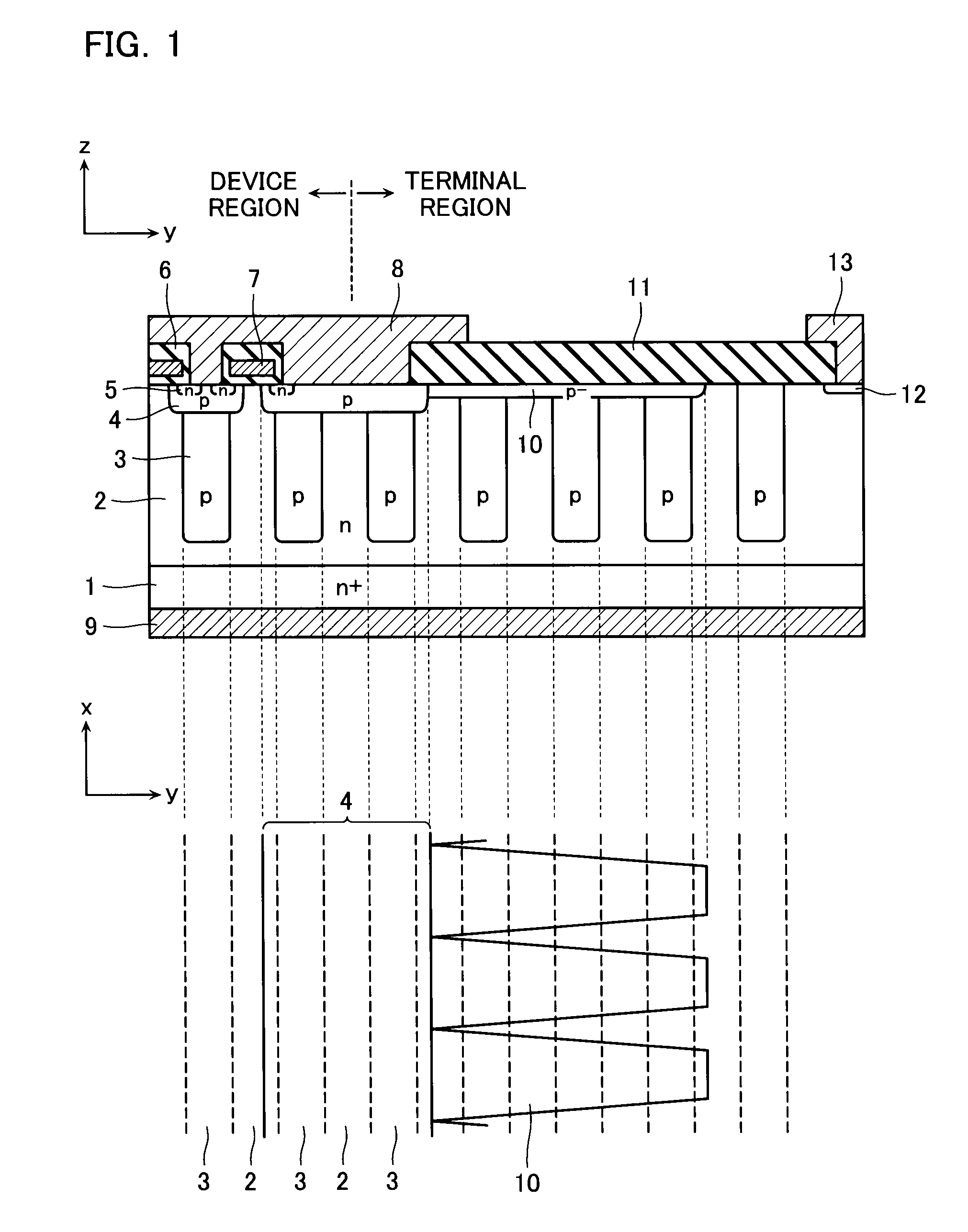
[0051]With reference to FIG. 8, a second embodiment of the present invention will now be described. FIG. 8 is a cross-sectional view and a plan view of the structure of a semiconductor device according to the second embodiment of the present invention. In FIG. 8, the upper portion is a cross-sectional view of the semiconductor device taken along the y-z plane. The lower portion in FIG. 8 is a plan view of the semiconductor device taken along the x-y plane. The semiconductor device in this embodiment in FIG. 8 has a configuration generally the same as that of the semiconductor device in the first embodiment. Accordingly, like elements are provided with like reference symbols and their description are omitted here.

[0052]In the device region and the terminal region of the semiconductor device in FIG. 8, the n and p type pillar regions 2 and 3 are alternately provided in a lateral direction, forming a stripe shape. The regions 2 and 3 comprise the super junction region. In the terminal ...

third embodiment

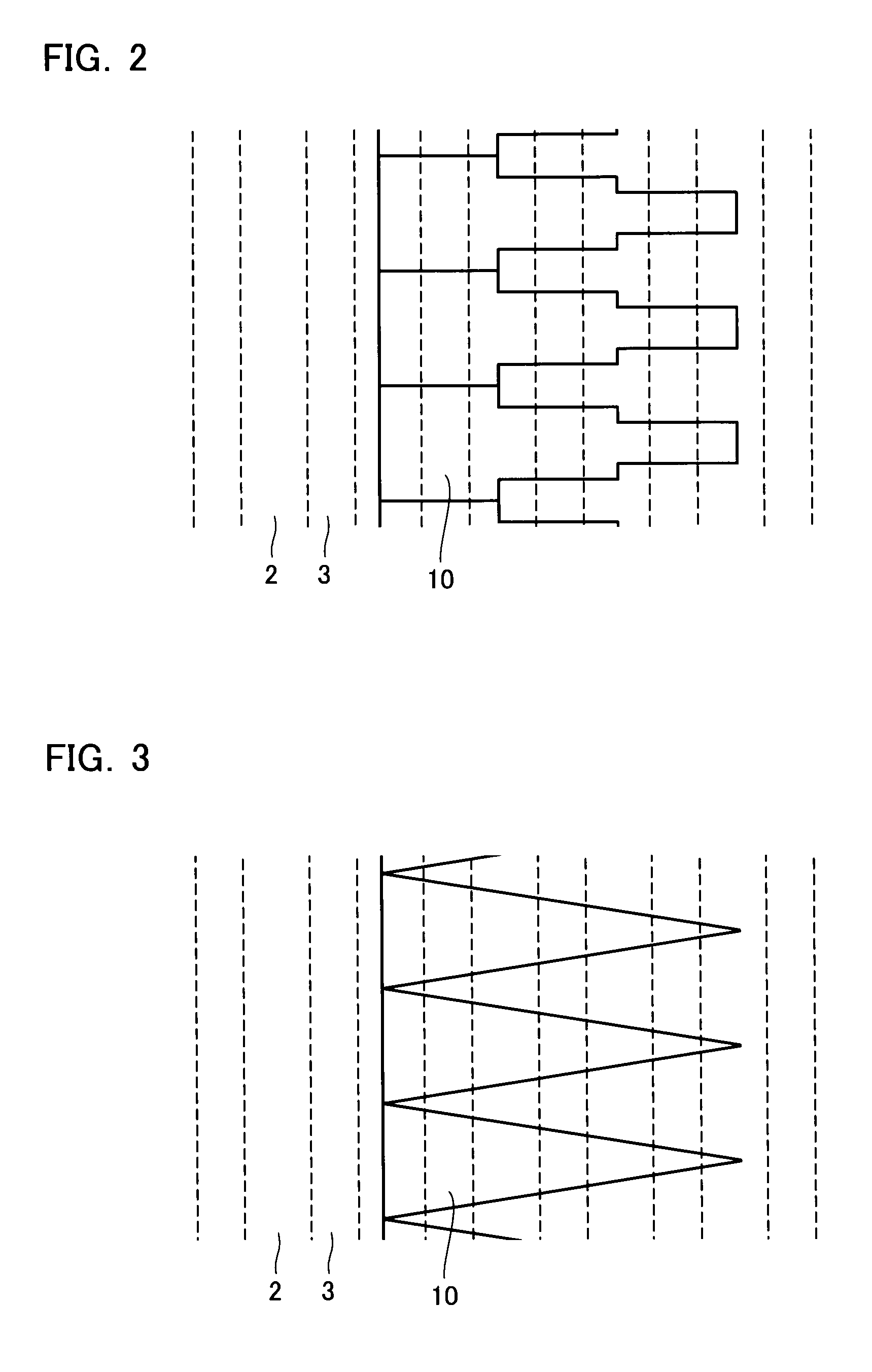
[0055]With reference to FIG. 9, a third embodiment of the present invention will now be described. FIG. 9 is a plan view of the structure of a semiconductor device according to the third embodiment of the present invention. The semiconductor device in this embodiment in FIG. 9 has a configuration generally the same as that of the semiconductor device in the first embodiment. Accordingly, like elements are provided with like reference symbols and their description are omitted here.

[0056]In the device region and the terminal region of the semiconductor device in FIG. 9, the n and p type pillar regions 2 and 3 are alternately provided in a lateral direction, forming a stripe shape. The regions 2 and 3 comprise the super junction region. The RESURF region 10 in the terminal region in this embodiment has a comb-like planar shape with repeatedly-formed teeth having tips facing the end portion of the terminal region. The tip of the teeth is forward tapered toward its tip. Each of the teeth...


PUM


Abstract

A semiconductor device includes an n+ type semiconductor substrate 1 and a super junction region that has, on the top of the substrate 1, an n and p type pillar regions 2 and 3 provided alternately. The device also includes, in the top surface of the super junction region, a p type base region 4 and an n type source layer 5. The device also includes a gate electrode 7 on the region 4 and layer 5 via a gate-insulating film 6, a drain electrode 9 on the bottom of the substrate 1, and a source electrode 8 on the top of the substrate 1. In the top surface of the super junction region in the terminal region, a RESURF region 10 is formed. The RESURF region has a comb-like planar shape with repeatedly-formed teeth having tips facing the end portion of the terminal region.

Description

CROSS REFERENCE TO RELATED APPLICATIONS[0001]This application is based on and claims the benefit of priority from prior Japanese Patent Application No. 2007-273430, filed on Oct. 22, 2007, the entire contents of which are incorporated herein by reference.BACKGROUND OF THE INVENTION[0002]1. Field of the Invention[0003]The present invention relates to a semiconductor device, and more particularly, to a semiconductor device including a super junction region.[0004]2. Description of the Related Art[0005]Vertical power metal oxide semiconductor field effect transistors (MOSFET) each have an ON-resistance that largely depends on the electrical resistance of the conductive layer (drift layer). The drift layer's electrical resistance depends on the impurity concentration thereof. A higher impurity concentration causes a lower ON-resistance. The higher impurity concentration, however, provides a lower breakdown voltage of the pn junction between the drift layer and the base layer. The impurit...

Claims


Application Information

Patent Timeline
Patent Type & Authority Patents(United States)
IPC IPC(8): H01L29/66
CPCH01L29/0615H01L29/0634H01L29/0696H01L29/7811H01L29/0638H01L29/1095H01L29/402H01L29/41741
Inventor SAITO, WATARUONO, SYOTAROIZUMISAWA, MASARUSUMI, YASUTOOHTA, HIROSHISEKINE, WATARUHATANO, NANA
Owner KK TOSHIBA
Why Eureka
Try Eureka