Clock power minimization with regular physical placement of clock repeater components

a clock repeater and clock power technology, applied in the field of semiconductor chips and integrated circuits, can solve the problems of large number of cells, difficult physical design without the aid of computers, and complicated connections between cells, and achieve the effect of reducing clock skew and improving clock power

US8010926B2Inactive Publication Date: 2011-08-30IBM CORP
10 Cites 15 Cited by

Patent Information

Authority / Receiving Office
US · United States
Patent Type
Patents(United States)
Current Assignee / Owner
Publication Date
2011-08-30
Estimated Expiration
Not applicable · inactive patent

Smart Images

  • Figure 1
    Figure 1
  • Figure 2
    Figure 2
  • Figure 3
    Figure 3
Patent Text Reader

Abstract

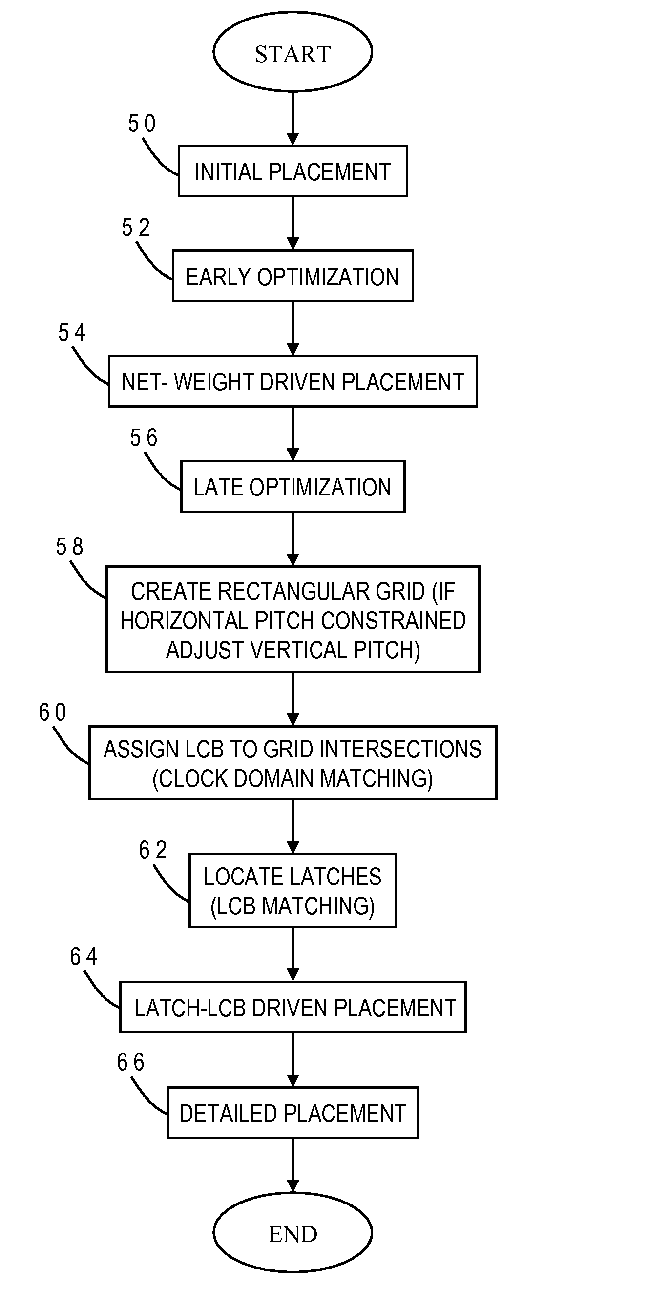
Power, routability and electromigration have become crucial issues in modern microprocessor designs. In high performance designs, clocks are the highest consumer of power. Arranging clocking components with regularity so as to minimize the capacitance on the clock nets can help reduce clock power, however, it may hurt performance due to some loss of flexibility in physically placing those components. The present invention provides techniques to optimally place clock components in a regular fashion so as to minimize clock power within a performance constraint. A rectangular grid is created and clock distribution structures are assigned to the grid intersection points. Latches are then located around the clock distribution structures to minimize an overall distance for connections between the latches and respective clock distribution structures. The horizontal and vertical pitches of the grid may be independently adjusted to achieve a more uniform spread of the clock distribution structures.
Need to check novelty before this filing date? Find Prior Art

Description

STATEMENT REGARDING FEDERALLY SPONSORED RESEARCH OR DEVELOPMENT

[0001] This invention was made with Government support under DARPA, HR0011-07-9-0002. THE GOVERNMENT HAS CERTAIN RIGHTS IN THIS INVENTION.BACKGROUND OF THE INVENTION

[0002] 1. Field of the Invention

[0003] The present invention generally relates to the fabrication and design of semiconductor chips and integrated circuits, and more particularly to a method of designing the physical layout (placement) of latches and other logic cells which receive clock signals from clock distribution structures such as local clock buffers.

[0004] 2. Description of the Related Art

[0005] Integrated circuits are used for a wide variety of electronic applications, from simple devices such as wristwatches to the most complex computer systems. A microelectronic integrated circuit (IC) chip can generally be thought of as a collection of logic cells with electrical interconnections between the cells, formed on a semiconductor substrate (e.g., silicon). A...

Examples

Embodiment Construction

)

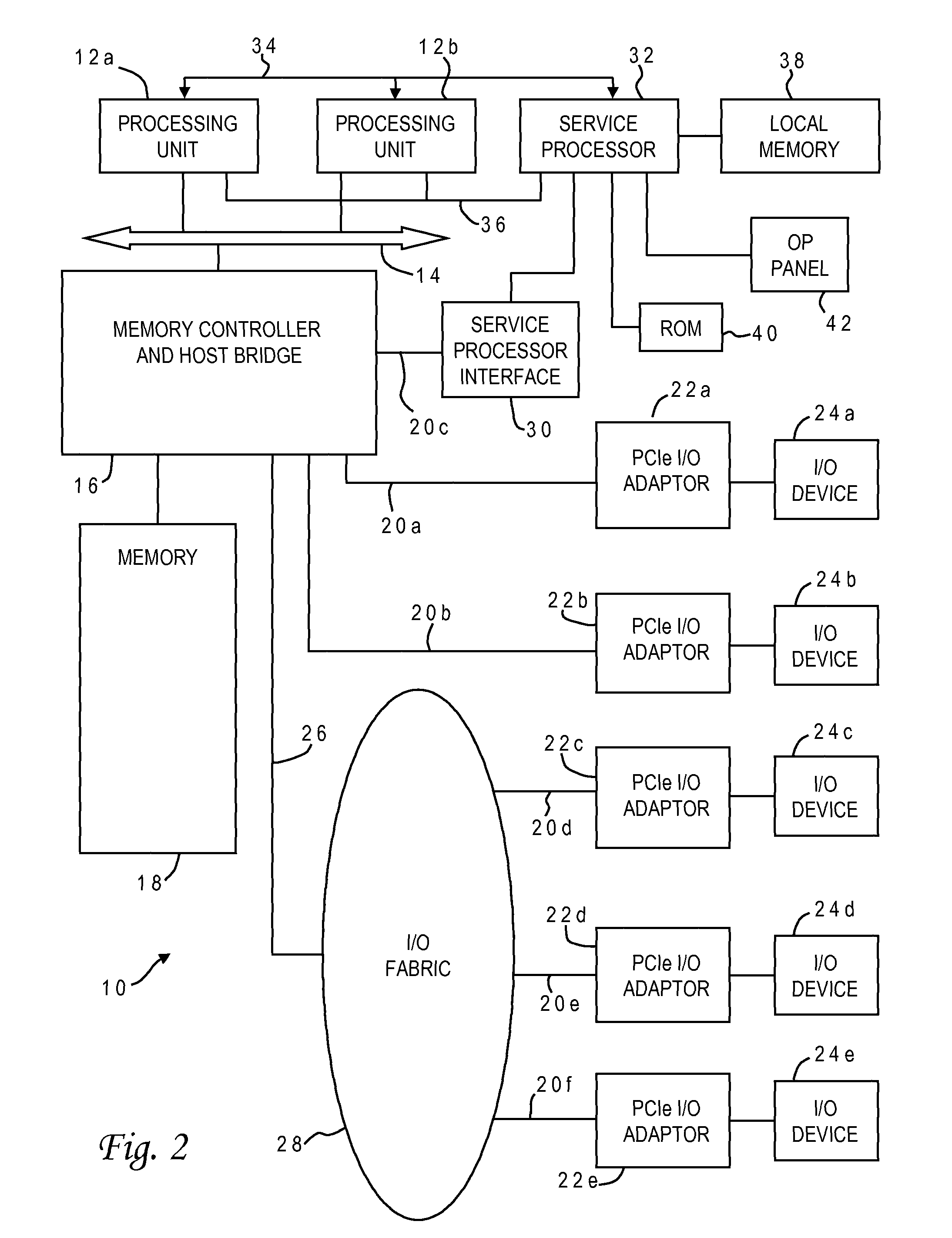
[0026]With reference now to the figures, and in particular with reference to FIG. 2, there is depicted one embodiment 10 of a computer system in which the present invention may be implemented. Computer system 10 is a symmetric multiprocessor (SMP) system having a plurality of processors 12a, 12b connected to a system bus 14. System bus 14 is further connected to a combined memory controller / host bridge (MC / HB) 16 which provides an interface to system memory 18. System memory 18 may be a local memory device or alternatively may include a plurality of distributed memory devices, preferably dynamic random-access memory (DRAM). There may be additional structures in the memory hierarchy which are not depicted, such as on-board (L1) and second-level (L2) or third-level (L3) caches.

[0027]MC / HB 16 also has an interface to peripheral component interconnect (PCI) Express links 20a, 20b, 20c. Each PCI Express (PCIe) link 20a, 20b is connected to a respective PCIe adaptor 22a, 22b, and each PC...