Resistance variable element and resistance variable memory apparatus

a resistance variable and memory apparatus technology, applied in digital storage, semiconductor devices, instruments, etc., can solve the problems of complex bidirectional current limiting elements, limited miniaturization of existing flash memory using floating gates, and difficult design of the relation between the resistance value of the resistance variable element and the resistance value of the bidirectional current limiting elemen

Inactive Publication Date: 2011-09-13
PANASONIC SEMICON SOLUTIONS CO LTD
View PDF12 Cites 101 Cited by
  • Summary
  • Abstract
  • Description
  • Claims
  • Application Information

AI Technical Summary

Benefits of technology

[0047]The present invention has the above configuration and the following effects. To be specific, the present invention can provide a new resistance variable element which can be manufactured at low temperature and has a feature that all the write voltage pulses have the same polarity as one another (i.e., the resistance variable element can be operated by unipolar drive), and a resistance variable memory apparatus using the resistance variable element.

Problems solved by technology

It is said that although there are such needs, there is a limit to miniaturization of an existing flash memory using a floating gate.
However, the bidirectional current limiting element is complex in configuration, and even in the case of using the bidirectional current limiting element, designing, for example, the relation between the resistance value of the resistance variable element and the resistance value of the bidirectional current limiting element is difficult.

Method used


Image

  • Resistance variable element and resistance variable memory apparatus
  • Resistance variable element and resistance variable memory apparatus
  • Resistance variable element and resistance variable memory apparatus

Examples


embodiment 1

[0084]Configuration

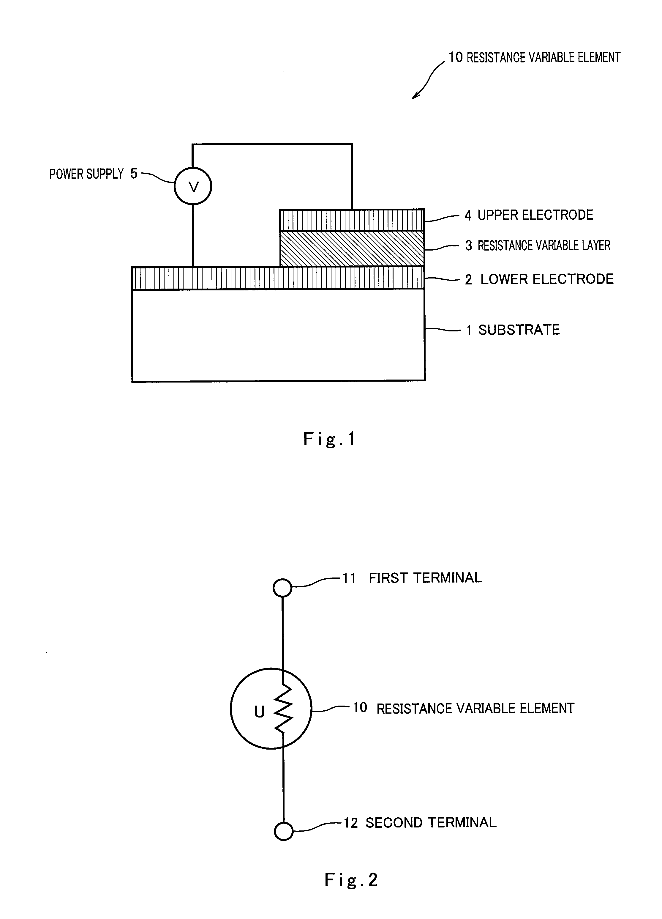
[0085]FIG. 1 is a schematic diagram showing one example of the configuration of a resistance variable element of Embodiment 1 of the present invention.

[0086]As shown in FIG. 1, a resistance variable element 10 of the present embodiment includes a substrate 1, a lower electrode 2 (first electrode) formed on the substrate 1, a resistance variable layer 3 formed on the lower electrode 2, and an upper electrode 4 (second electrode) formed on the resistance variable layer 3. The lower electrode 2 and the upper electrode 4 are electrically connected to the resistance variable layer 3. Note that the upper electrode 4 may be the first electrode, and the lower electrode 2 may be the second electrode.

[0087]The substrate 1 is constituted by a silicon substrate for example.

[0088]Each of the lower electrode 2 and the upper electrode 4 can be constituted by, for example, using one or a plurality of materials selected from the group consisting of Ag (silver), Au (gold), Pt (plat...

example 1

[0123]A lower electrode (20 μm×20 μm) made of Pt was formed on a silicon substrate by sputtering so as to have a thickness of 0.2 μm. A target of ZnFe2O4 and a target of Fe3O4 were prepared, and those targets were caused to electrically discharge at the same time by sputtering. Using masking and lithography, a resistance variable layer (10 μm ×10 μm, 100 μm2) having the spinel structure represented by the chemical formula of (ZnxFe1-x)Fe2O4 was formed on the lower electrode. The temperature of the substrate when forming the resistance variable layer was 300° C. The size of a contact portion where the lower electrode and the resistance variable layer contact each other was 2 μm×2 μm (4 μm2). The thickness of the resistance variable layer was 100 nm. Further, an upper electrode (2 μm×2 μm) made of Pt was formed on the resistance variable layer by sputtering using masking and lithography so as to have a thickness of 0.2 μm. Thus, the resistance variable element was obtained. A contact ...

example 2

[0130]In Example 2, the resistance variable element was formed by the same method as Example 1 except that a parameter was different. Using this resistance variable element, the writing and the reading were carried out.

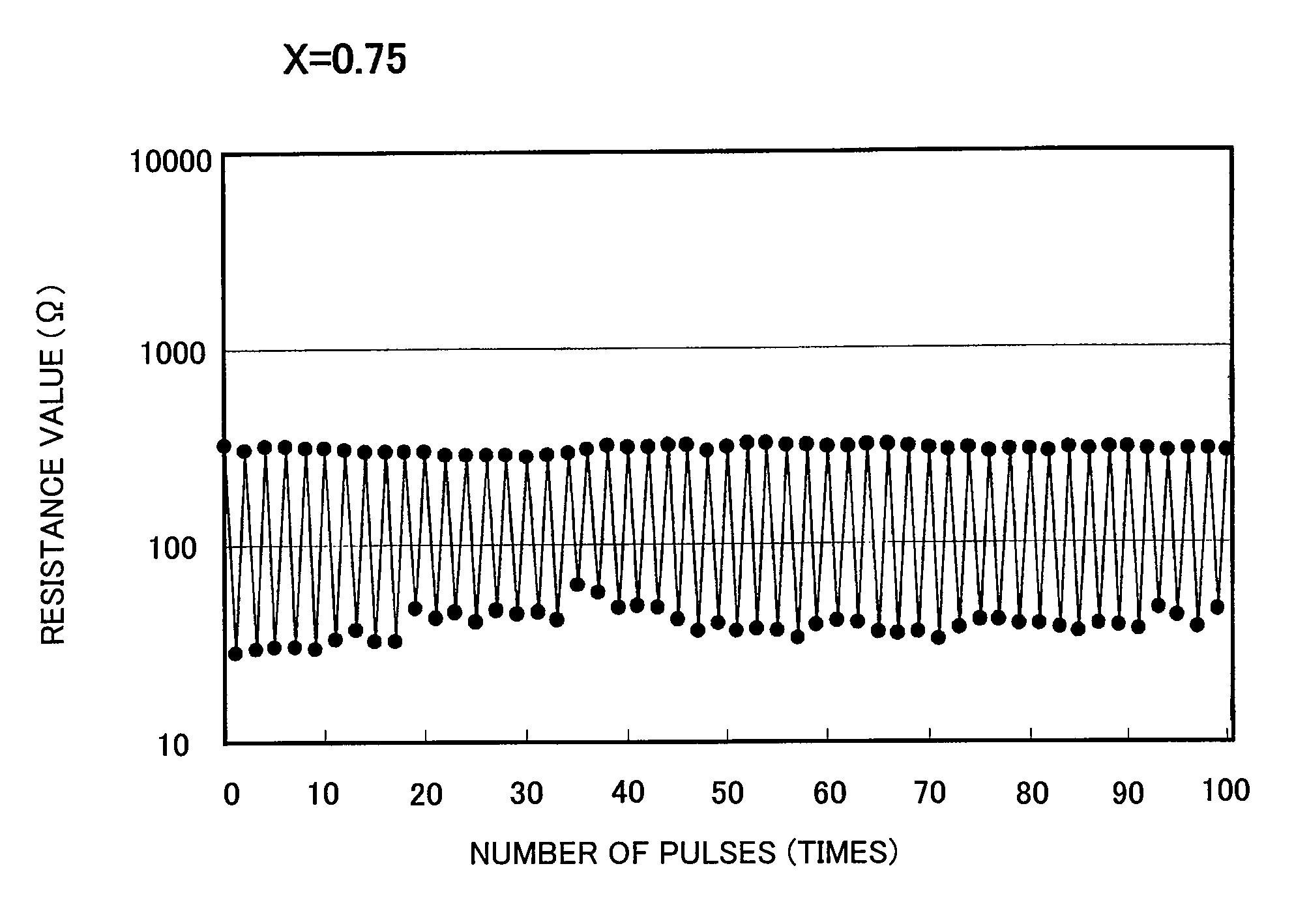
[0131]To be specific, in Example 2, the voltage applied to each target was adjusted such that the value of X of (ZnxFe1-x)Fe2O4 constituting the resistance variable layer became 0.75. The value of X was verified by the combination of RBS (Rutherford backscattering) and fluorescent X-ray analysis. As a result of this verification, the value of X was 0.75.

[0132]It was confirmed that the resistance variable element of Example 2 was nonvolatile, i.e., the resistance value of the resistance variable element of Example 2 did not change even if the power supply was turned off.

[0133]FIG. 8 is a diagram showing changes in resistance value when the voltage pulses are applied to the resistance variable element of Example 2. As shown in FIG. 8, the resistance state changed from t...


PUM


Abstract

A resistance variable element of the present invention and a resistance variable memory apparatus using the resistance variable element are a resistance variable element (10) including a first electrode, a second electrode, and a resistance variable layer (3) provided between the first electrode (2) and the second electrode (4) to be electrically connected to the first electrode (2) and the second electrode (4), wherein the resistance variable layer (3) contains a material having a spinel structure represented by a chemical formula of (ZnxFe1-x)Fe2O4, and the resistance variable element (10) has a feature that an electrical resistance between the first electrode (2) and the second electrode (4) increases by applying a first voltage pulse to between the first electrode (2) and the second electrode (4), and the electrical resistance between the first electrode (2) and the second electrode (4) decreases by applying a second voltage pulse whose polarity is the same as the first voltage pulse to between the first electrode (2) and the second electrode (4), and a resistance variable memory apparatus using the resistance variable element (10).

Description

RELATED APPLICATIONS[0001]This application is the U.S. National Phase under 35 U.S.C. §371 of International Application No. PCT / JP2007 / 074556, filed on Dec. 20, 2007, which in turn claims the benefit of Japanese Application No. 2006-354218, filed on Dec. 28, 2006, the disclosures of which Applications are incorporated by reference herein.TECHNICAL FIELD[0002]The present invention relates to a resistance variable element and a resistance variable memory apparatus, and more particularly to a resistance variable element whose electrical resistance changes depending on a voltage pulse applied thereto, and a resistance variable memory apparatus utilizing the resistance variable element.BACKGROUND ART[0003]As digital technologies of electronic devices progress, in order to save data, such as images, there are growing needs for an increase in capacity of a nonvolatile resistance variable element, a reduction in electric power required for writing to the nonvolatile resistance variable elem...

Claims


Application Information

Patent Timeline
Patent Type & Authority Patents(United States)
IPC IPC(8): G11C11/00
CPCG11C13/0007H01L45/1625H01L45/04H01L45/1233H01L45/147H01L27/2409G11C2213/31G11C2213/72H10B63/20H10N70/20H10N70/8836H10N70/026H10N70/826
Inventor MURAOKA, SHUNSAKUOSANO, KOICHIFUJII, SATORU
Owner PANASONIC SEMICON SOLUTIONS CO LTD
Why Eureka
Try Eureka