Planar waveguide lens design

a waveguide and lens design technology, applied in the direction of optical waveguide light guide, instruments, computing, etc., can solve the problems of affecting the accuracy of inter-layer registration, and being difficult to control, so as to improve the mechanical robustness, less susceptible to stray light, and the effect of reducing the risk of light escaping

Inactive Publication Date: 2011-11-22
ZETTA RES & DEV LLC RPO SERIES
View PDF23 Cites 157 Cited by
  • Summary
  • Abstract
  • Description
  • Claims
  • Application Information

AI Technical Summary

Benefits of technology

[0042]Advantageously, optical elements according to at least a preferred embodiment of the present invention are more mechanically robust, easier to incorporate into the touch screen assembly and are less susceptible to stray light and the ingress of foreign matter.

Problems solved by technology

On the receive side however, the problem is potentially more serious because of the possibility of out-of-plane stray light entering the receive elements (this effect can be seen by reversing the direction of light rays 25 in FIG. 2b)
However for reasons of cost, it may be preferable to use plastic substrates, and unlike silicon where the only dimensional variable is thermal expansion (which is relatively easy to control), the dimensions of plastic substrates are also known to depend on humidity and thermal and mechanical history, which are far more difficult to control.
For these reasons, accurate inter-layer registration is a known problem in the fabrication of multilayer plastic devices such as flexible displays.
Yet another problem with the transmit and receive elements of the existing design is that curved end face 21, being a reflective surface, must be an interface with a large refractive index difference, such as an air / polymer interface.
However there is then a risk that the exposed curved end face could be damaged, for example during assembly of the optical touch screen sensor.

Method used


Image

  • Planar waveguide lens design
  • Planar waveguide lens design
  • Planar waveguide lens design

Examples


example 1

[0071]Following the procedure disclosed in U.S. Pat. No. 6,818,721, a lower refractive index polymer A was prepared with a viscosity of 2500 cP (at 20° C.) and a refractive index (measured at 20° C. on an Abbé refractometer with room light) of 1.483. A higher refractive index polymer B was prepared with a viscosity of 2200 cP (at 20° C.) and a refractive index of 1.509 (at 20° C.). A suitable photoinitiator was added to both polymer A and polymer B

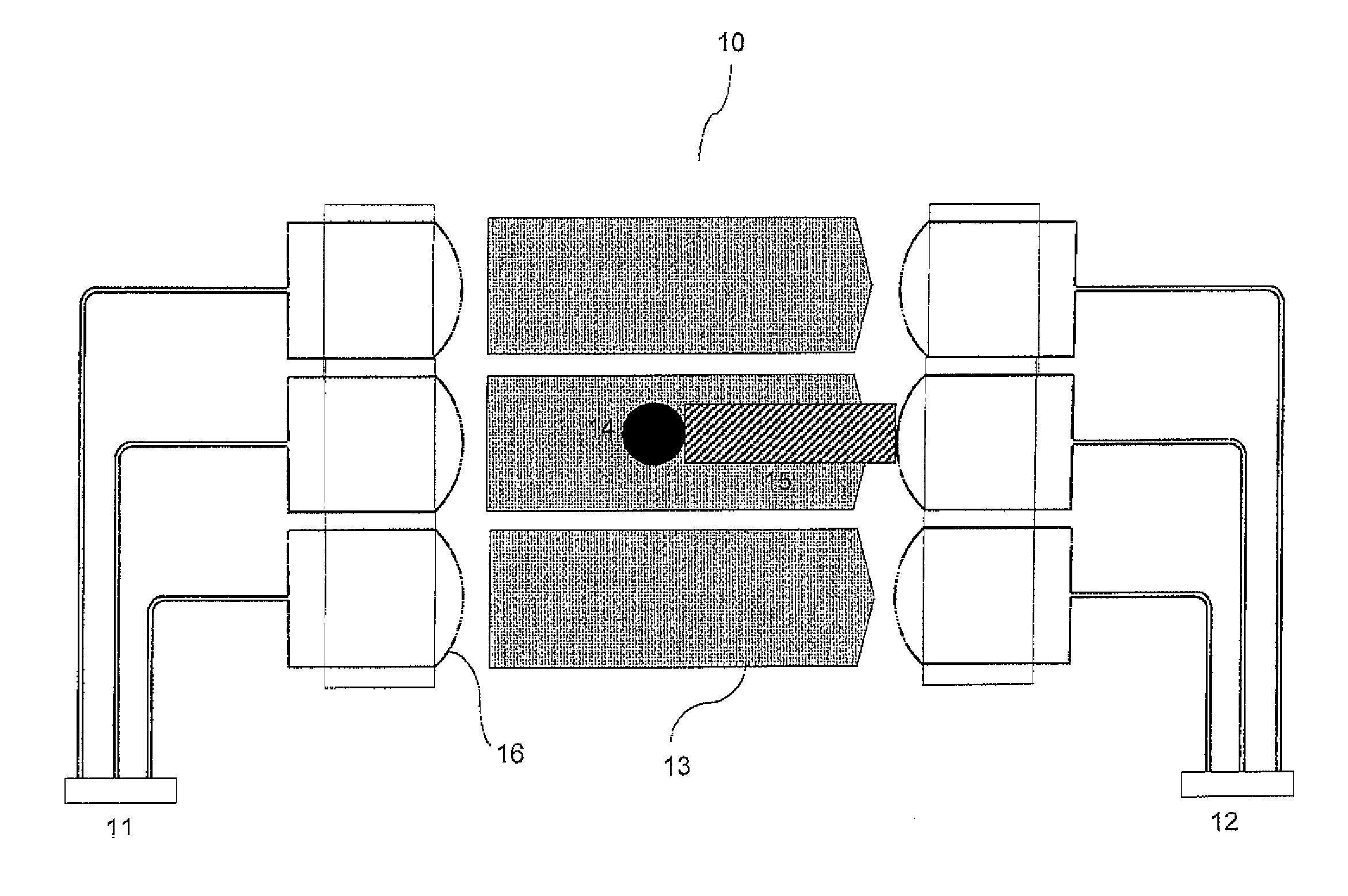
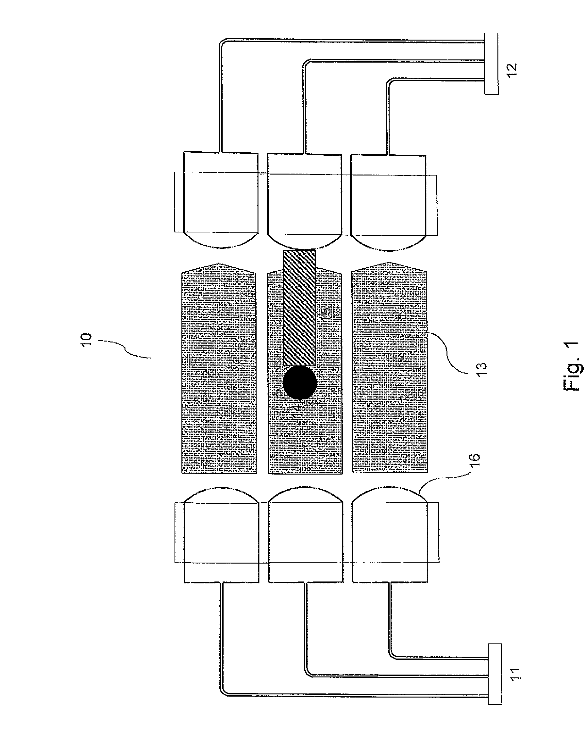
[0072]Polymer A was spin coated onto silicon wafer 40 and cured with UV light from a mercury lamp, to form lower cladding layer 41 with thickness 20 μm and refractive index 1.485 (at 20° C. and 850 nm). Polymer B was spin coated onto lower cladding layer 41 to form core layer 42, and patterned with UV light through a mask. The unexposed polymer B material was then dissolved in isopropanol to form input waveguide 31 and transmit element 30 incorporating converging lens 35 composed of air. Exposed core layer 42 had thickness of 11 μm and a r...

example 2

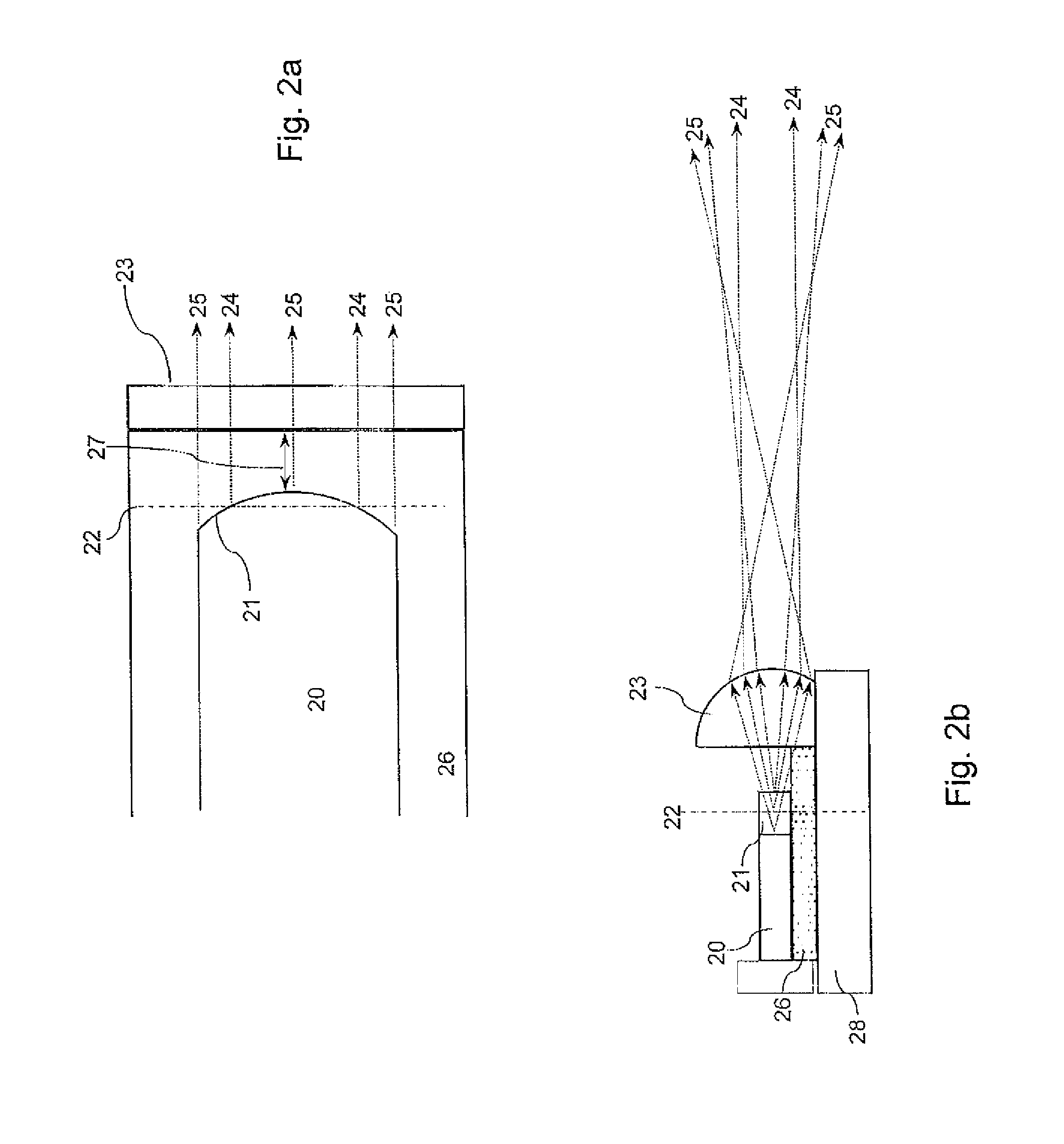
[0076]FIG. 5 shows a transmit element 30 according to the first embodiment of the invention, containing a plano-concave lens 50 comprising a concave front surface 51 and a planar back surface 52. In this example, plano-concave lens 50 is composed of air and extends across the full width of polymer slab waveguide region 33, thereby splitting it into first slab waveguide region 53 and second slab waveguide region 54. Such a design may be advantageous for a wet development fabrication process, to aid the passage of solvent and the removal of unexposed material. It will be appreciated that second slab waveguide region 54 allows end face 38 to be straight but has no focusing function, and can therefore be of any length. For example it may be made arbitrarily short to minimise the overall length of transmit element 30. In practice, second slab waveguide region 54 should have a length 55 of at least 30 μm, to allow sufficient margin for the dicing process that forms end face 38. To minimis...

example 3

[0079]FIG. 7 shows another transmit element 30 according to a first embodiment of the invention, containing bi-concave lens 70 composed of air and comprising concave front surface 71 and concave back surface 72. Bi-concave lens 70 extends across the full width of polymer slab waveguide region 33, splitting it into first slab waveguide region 73 and second slab waveguide region 74. Concave front surface 71 is designed to be an are of a circle centred on point 34, so that light rays emanating from this point encounter front surface 71 at normal incidence and pass through without being refracted. The light rays then encounter concave back surface 72, which is designed to collimate them into output rays 75. In another well known result of geometrical optics (“Optics”, E. Hecht, 2nd ed, Addison-Wesley (1987), p. 129-132), if light rays emanating from a point source in a medium of lower refractive index n1 pass into a medium of higher refractive index n2 through a hyperboloidal interface,...


PUM


Abstract

This invention relates to an improved design for the transmit and receive optical elements of a waveguide-based optical touch screen sensor, where at least one converging lens is incorporated within the body of each transmit and receive element. The optical elements of the improved design are more mechanically robust, easier to incorporate into the touch screen assembly, and are less susceptible to stray light and the ingress of foreign matter. In one embodiment the converging lens collimates the light into a plane wave. In another embodiment the converging lens focuses the light to an external point. In yet another embodiment, each transmit and receive element also includes at least one diverging lens. The transmit and receive elements and associated waveguides preferably comprise photo-patternable polymers.

Description

FIELD OF THE INVENTION[0001]This invention relates to improved designs for transmit and receive optical elements of a waveguide-based optical touch screen sensor.BACKGROUND TO THE INVENTION[0002]Any discussion of the prior art throughout the specification should in no way be considered as an admission that such prior art is widely known or forms part of common general knowledge in the field.[0003]FIG. 1 illustrates the operation of an optical touch screen sensor 10 described in U.S. Pat. Nos. 5,914,709, 6,181,842 and 6,351,260, and U.S. Patent Application Nos. 2002 / 0088930 A1 and 2004 / 0201579 A1 (the contents of which are incorporated into this specification by way of cross-reference). In this optical touch screen sensor design, integrated optical waveguides 11, 12 are used to launch an array of light beams 13 across a screen, then collect them at the other side of the screen and conduct them to a position-sensitive detector A touch event 14 (eg by a finger or stylus) is detected as...

Claims


Application Information

Patent Timeline
Patent Type & Authority Patents(United States)
IPC IPC(8): G02B6/10G02B6/32G02B6/34G02B6/42G02B27/10G02B6/26G06F3/033G06F3/042
CPCG02B6/12004G02B6/1221G02B6/138G02B27/30G06F3/0421G02B6/32G02B2006/12102G02B2006/1219
Inventor ATKINS, GRAHAM ROYKUKULJ, DAXCHARTERS, ROBERT BRUCE
Owner ZETTA RES & DEV LLC RPO SERIES
Why Eureka
Try Eureka