Unlock instant, AI-driven research and patent intelligence for your innovation.

Plasma display device and driving method thereof

a technology of display device and driving circuit, which is applied in the direction of electric digital data processing, instruments, computing, etc., can solve the problems of current stressing the driving circuit, and achieve the effects of reducing or preventing deterioration, reducing or preventing the deterioration of components, and relieving current stress from a driving circui

Inactive Publication Date: 2012-02-14
SAMSUNG SDI CO LTD
View PDF3 Cites 0 Cited by
  • Summary
  • Abstract
  • Description
  • Claims
  • Application Information

AI Technical Summary

Benefits of technology

The solution effectively reduces current stress on the driving circuit and prevents overcurrent, improving the reliability and longevity of the plasma display device components.

Problems solved by technology

In the case of the reset waveform, its voltage falls from a very high electric potential to a ground electric potential or an electric potential close to ground, so the difference between the starting electric potential and the ending electric potential of the scan electrode during the time its voltage falls is very large, causing a problem in that its current can stress the driving circuit.

Method used


Image

  • Plasma display device and driving method thereof
  • Plasma display device and driving method thereof
  • Plasma display device and driving method thereof

Examples


Embodiment Construction

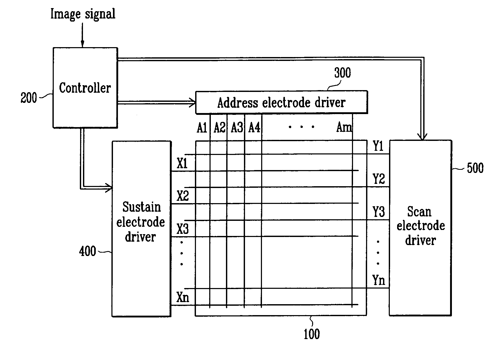
[0045]Hereinafter, embodiments of the present invention will be described with reference to the accompanying drawings so that those skilled in the art to which the present invention pertains can easily carry out the present invention. However, the present invention may be modified in many different forms and it should not be limited to the embodiments set forth herein. Also, in the context of the present application, when an element is referred to as being “coupled to” another element, it can be directly coupled to the another element or be indirectly coupled to the another element with one or more intervening elements interposed therebetween. Like reference numerals designate like elements throughout the specification.

[0046]In order to reduce or prevent a current stress associated with the ramping voltage, the present applicant has previously proposed the improved technique of Korean Patent Application No. 10-2004-0095008. However, although the improved technique disclosed there ha...


PUM


Abstract

A plasma display device and a method of driving the same, capable of reducing or preventing the deterioration of components such as a switching device, due to an overcurrent. In a reset period, in order to cause the voltage of a scan electrode to ramp down from a first voltage to a second voltage, a panel driver includes a falling ramp switch that repeats turn-on / turn-off operations, alternately coupling and de-coupling a low-level power supply to the scan electrode, resulting in a gradually falling ramp waveform. A switch controller generates a switching pulse to control the falling ramp switch. Each turn-on time of the switching pulse for the initial falling ramp waveform following a power-on of the plasma display device is controlled to be shorter than each turn-on time of the switching pulse for other falling ramp waveform.

Description

CROSS-REFERENCE TO RELATED APPLICATION[0001]This application claims priority to and the benefit of Korean Patent Application No. 10-2007-0049621, filed on May 22, 2007, in the Korean Intellectual Property Office, the entire content of which is incorporated herein by reference.BACKGROUND[0002]1. Field of the Invention[0003]The present invention relates to a plasma display device and a method of driving the same.[0004]2. Discussion of Related Art[0005]A plasma display device is a flat panel display device that can display characters or images using a gas discharge plasma wherein, according to the size of the display panel, more than several hundreds of thousands to several millions of pixels are arranged in a matrix format.[0006]A conventional plasma display device is driven by dividing one image frame into a plurality of subfields, and gray levels are displayed by the combination of the subfields. Each subfield includes a reset period, an address period, and a sustain period.[0007]As...

Claims


Application Information

Patent Timeline
Patent Type & Authority Patents(United States)
IPC IPC(8): G09G3/28
CPCG09G3/2927G09G3/2965G09G2310/066G09G2330/025G09G3/296
Inventor KAZUHIRO, ITOSONG, YOO-JINKIM, TAE-WOOK
Owner SAMSUNG SDI CO LTD