
Organic light emitting diode display device

a light-emitting diode and display device technology, applied in the direction of instruments, discharge tubes luminescnet screens, optical elements, etc., can solve the problems of large loss of light generated by organic emission layers, poor black color expression and contrast etc., to improve the viewing angle of light, effectively suppressing external light reflection, the effect of improving the visual effect of oled display devices

Active Publication Date: 2012-02-28
SAMSUNG DISPLAY CO LTD
View PDF17 Cites 1 Cited by
  • Summary
  • Abstract
  • Description
  • Claims
  • Application Information

AI Technical Summary

Benefits of technology

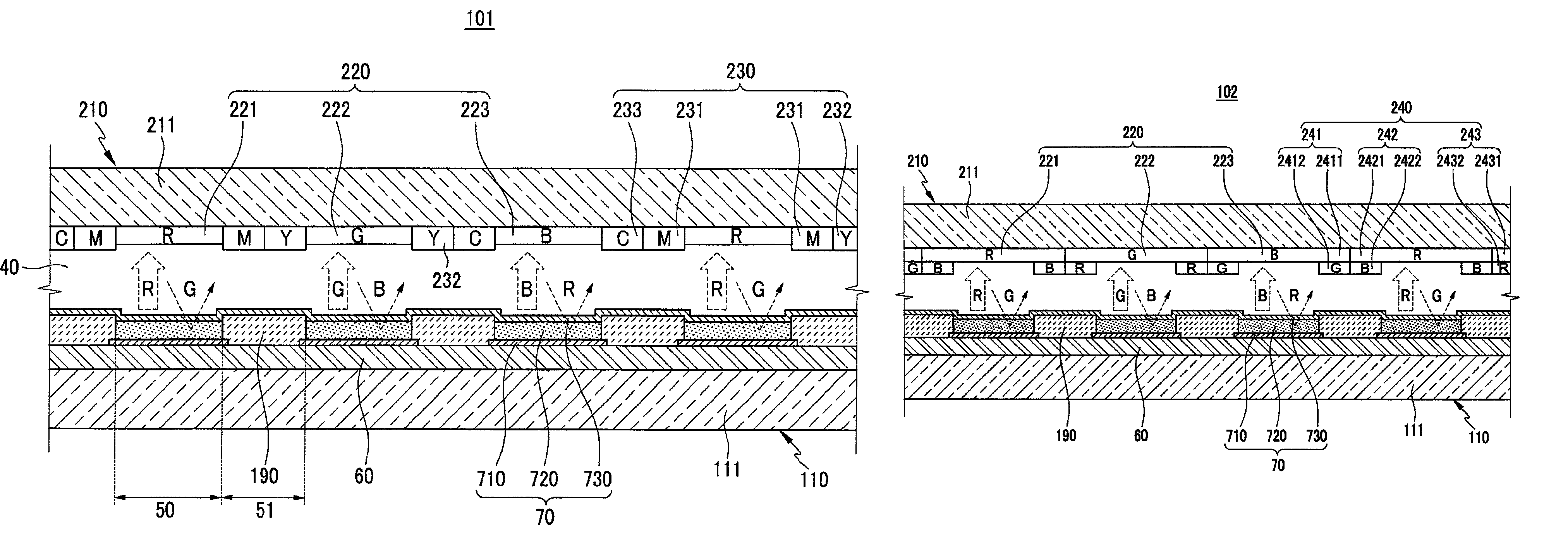
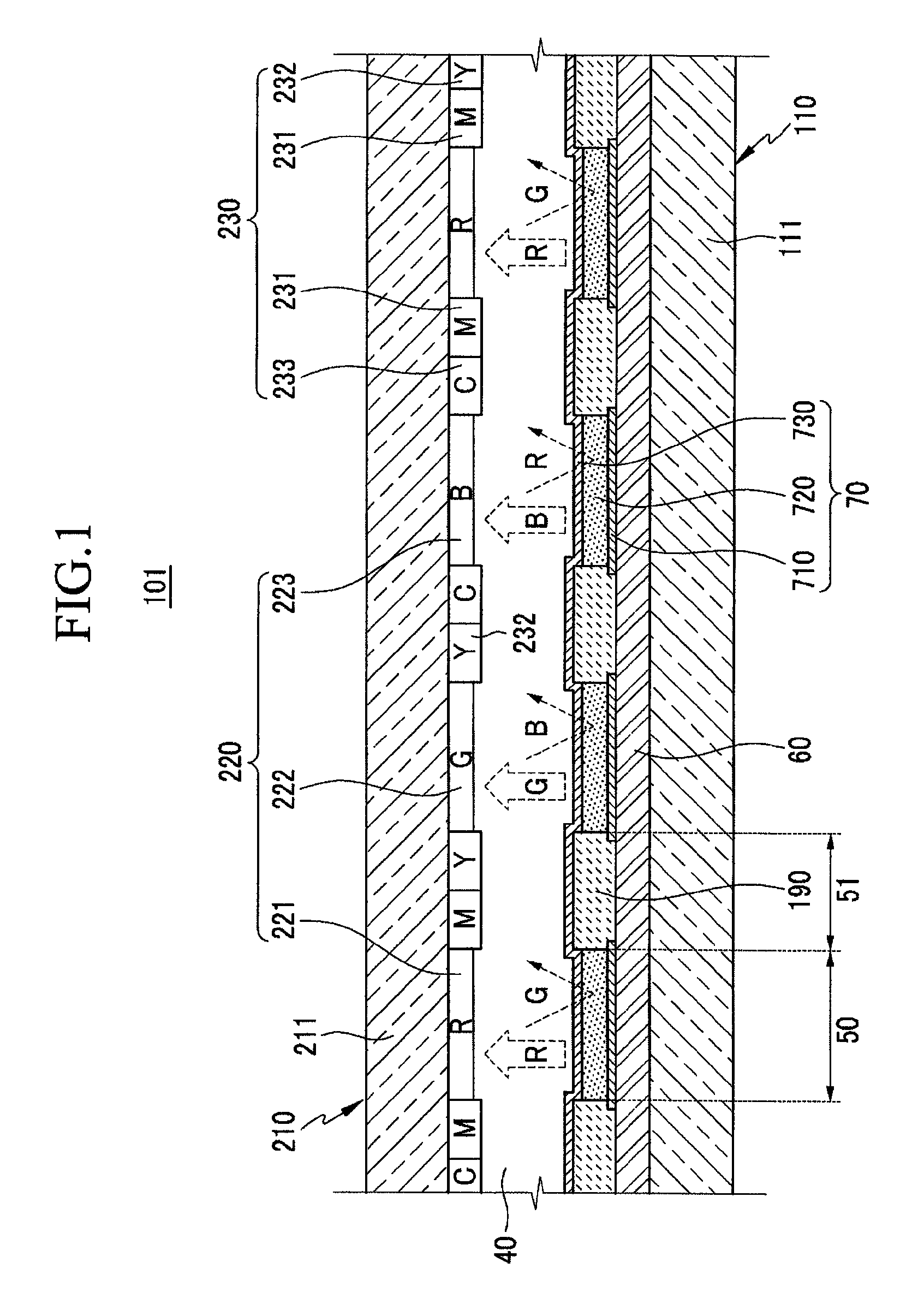
[0009]It is therefore an aspect of the present invention to provide an improved organic light emitting diode (OLED) display device to improve visibility by suppressing reflection of external light and to minimize loss of light emitted by the organic light emitting element.
[0029]According to the exemplary embodiment of the present invention, visibility of the OLED display device can be improved by effectively suppressing reflection of external light, and by minimizing the light loss emitted outside from the organic light emitting element.
[0030]Further, the OLED display device can have an improved light viewing angle.

Problems solved by technology

Thus, when the OLED display device is used in a bright environment, the black color expression and the contrast of the OLED display device become poor due to the reflection of external light incident from the exterior of the OLED display device.
A contemporary method that suppresses reflection of external light through the polarizing plate and the phase delay plate however has a problem where a large amount of light generated from an organic emission layer may also be lost when the light generated from an organic emission layer is emitted to the exterior of the OLED display device by the polarizing plate and the phase delay plate.

Method used


Image

  • Organic light emitting diode display device
  • Organic light emitting diode display device
  • Organic light emitting diode display device

Examples


Embodiment Construction

[0037]The present invention will be described more fully hereinafter with reference to the accompanying drawings, in which exemplary embodiments of the invention are shown. As those skilled in the art would realize, the described embodiments may be modified in various different ways, all without departing from the spirit or scope of the present invention.

[0038]Furthermore, with exemplary embodiments of the present invention, detailed description is given for the constituent elements in the first exemplary embodiment with reference to the relevant drawings by using the same reference numerals for the same constituent elements, while only different constituent elements from those related to the first exemplary embodiment are described in other exemplary embodiments.

[0039]Parts that are irrelevant to the description are omitted in order to clearly describe the present invention, and like reference numerals designate like elements throughout the specification.

[0040]Furthermore, as the s...


PUM


Abstract

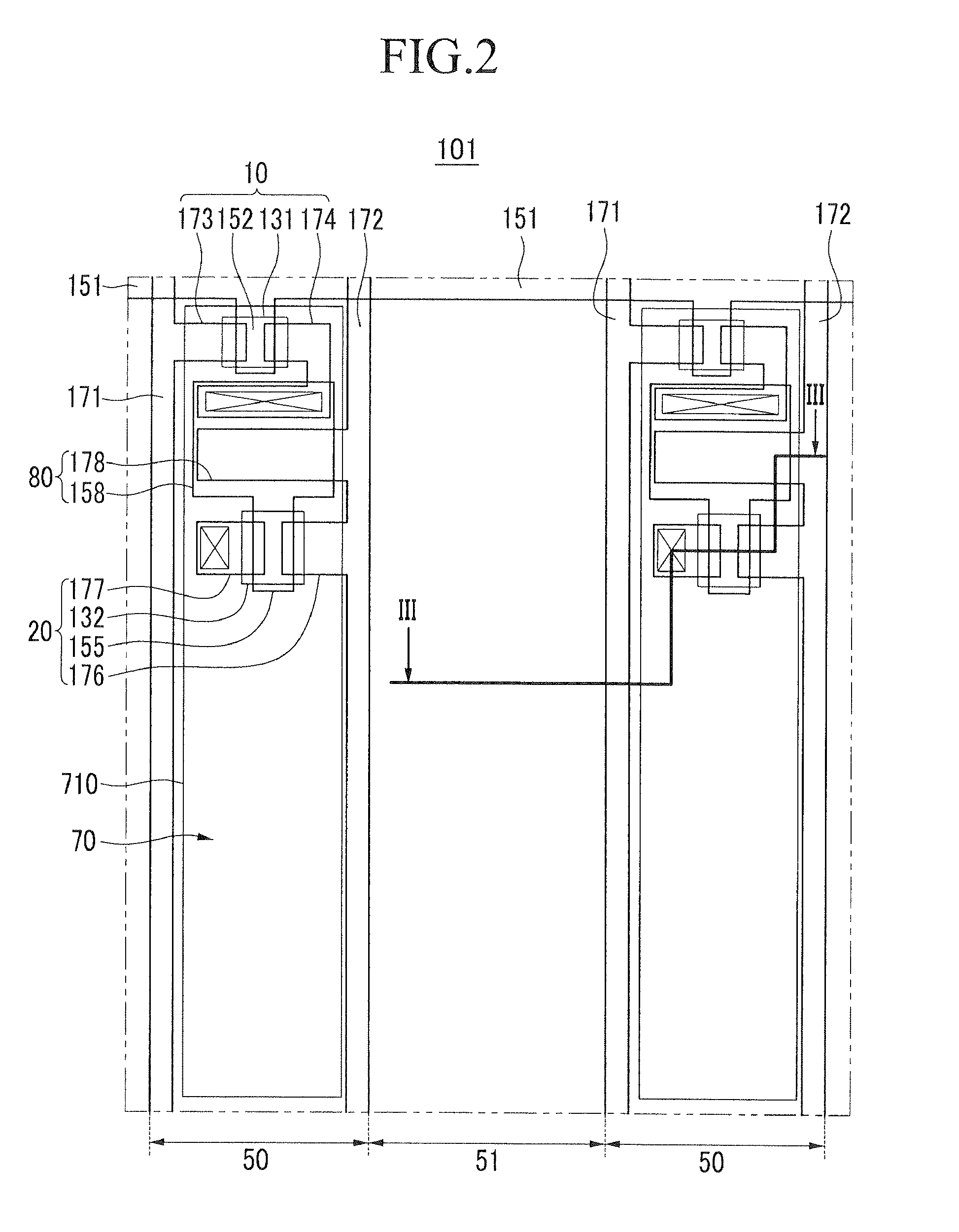
An organic light emitting diode (OLED) display device includes a first substrate main body divided into a plurality of pixel areas, and a non-pixel area respectively disposed between each of the plurality of pixel areas; a plurality of organic light emitting elements formed in each of the plurality of pixel areas; a second substrate main body disposed to face to the plurality of organic light emitting elements with a vacuumed space therebetween; and a selective light absorbing layer formed on a major surface of the second substrate main body and the selective light absorbing layer facing toward the non-pixel area, and the selective light absorbing layer selectively absorbing light of a color that corresponds to a major color component among color components of external incident light reflected at one of the plurality of organic light emitting elements neighboring the non-pixel area.

Description

CLAIM OF PRIORITY[0001]This application makes reference to, incorporates the same herein, and claims all benefits accruing under 35 U.S.C. §119 from an application earlier filed in the Korean Intellectual Property Office on 28 Jul. 2009 and there duly assigned Serial No. 10-2009-0069060.BACKGROUND OF THE INVENTION[0002]1. Field of the Invention[0003]The present invention relates to an organic light emitting diode (OLED) display device. More particularly, the present invention relates to an OLED display device of which a display characteristic is improved by efficiently suppressing reflection of external light.[0004]2. Description of the Related Art[0005]An organic light emitting diode (OLED) display device is a self emissive display device that displays images by using organic light emitting diodes, and has a relatively smaller thickness and lighter weight compared to a LCD device, because the OLED display device differs from a liquid crystal display (LCD) device in that the OLED di...

Claims


Application Information

Patent Timeline
Patent Type & Authority Patents(United States)
IPC IPC(8): H01J1/62
CPCH01L51/5284H01L27/3211H01L27/3244H10K59/35H10K59/12H10K50/865G02B5/22
Inventor PARK, SOON-RYONGJEONG, HEE-SEONGJUNG, WOO-SUK
Owner SAMSUNG DISPLAY CO LTD
Learn More