Release surfaces, particularly for use in nanoimprint lithography

a technology of release surfaces and nanoimprints, applied in the field of lithography, can solve the problems of high cost of x-ray lithography tools, economic impracticality of using these technologies for mass production of sub-50 nm structures, and inability to meet the requirements of high-speed lithography, so as to improve the resolution of images, eliminate many resolution limitations, and use more often

Inactive Publication Date: 2012-03-06
RGT UNIV OF MINNESOTA
View PDF17 Cites 4 Cited by
  • Summary
  • Abstract
  • Description
  • Claims
  • Application Information

AI Technical Summary

Benefits of technology

[0009]The present invention relates to a method and apparatus for performing ultra-fine line lithography of the type used to produce integrated circuits and microdevices. A layer of thin film is deposited upon a surface of a substrate. A mold having its mold surface treated with the release materials of the present invention and at least one protruding feature and a recess is molded into the thin film, therefore the thickness of the film under the protruding feature is thinner than the of the film under the recess and a relief is formed in the thin film. The relief generally conforms to the shape of the feature on the mold. After the mold is removed from the film, the thin film is processed such that the thinner portion of the film in the relief is removed, exposing the underlying substrate. Thus, the pattern in the mold is replicated in the thin film, completing the lithography. The patterns in the thin film will be, in subsequent processes, reproduced in the substrate or in another material that is added onto the substrate. The use of the release treatment on the mold surface enhances the resolution of the image and can protect the mold so that it can be used more often without showing wear on fine features in the mold.
[0010]The invention described here is based on a fundamentally different principle from conventional lithography. The process invention can eliminate many resolution limitations imposed in conventional lithography, such as wavelength limitation, backscattering of particles in the resist and substrate, and optical interference. It has been demonstrated the present invention can include a high throughput mass production lithography method for generating sub-25 nm features. Furthermore, the present invention has the ability to mass produce sub-10 nm features at a low cost. These capabilities of the present invention is unattainable with the prior art, and the use of the adherent release property coating improves the durability and the resolution of the process even further. The present process, however, has implications and utility for more macroscopic details in molding surfaces and would include features in the 50 nm range, the super-100 nm range, and the super 200 nm range, as well as macroscopic dimensions in the visual range of features (e.g. 0.1 mm and greater).

Problems solved by technology

Numerous technologies have been developed to service these needs, but they all suffer serious drawbacks and none of them can mass produce sub-50 nanometer features at a low cost.
However, using these technologies for mass production of sub-50 nm structures seems economically impractical due to inherent low throughput in a serial processing tool.
But X-ray lithography tools are expensive and their ability for mass producing sub-50 nm structures is yet to be commercially demonstrated.
However, the practicality of such lithography in a manufacturing tool is hard to judge at this point.

Method used


Image

  • Release surfaces, particularly for use in nanoimprint lithography
  • Release surfaces, particularly for use in nanoimprint lithography
  • Release surfaces, particularly for use in nanoimprint lithography

Examples


Embodiment Construction

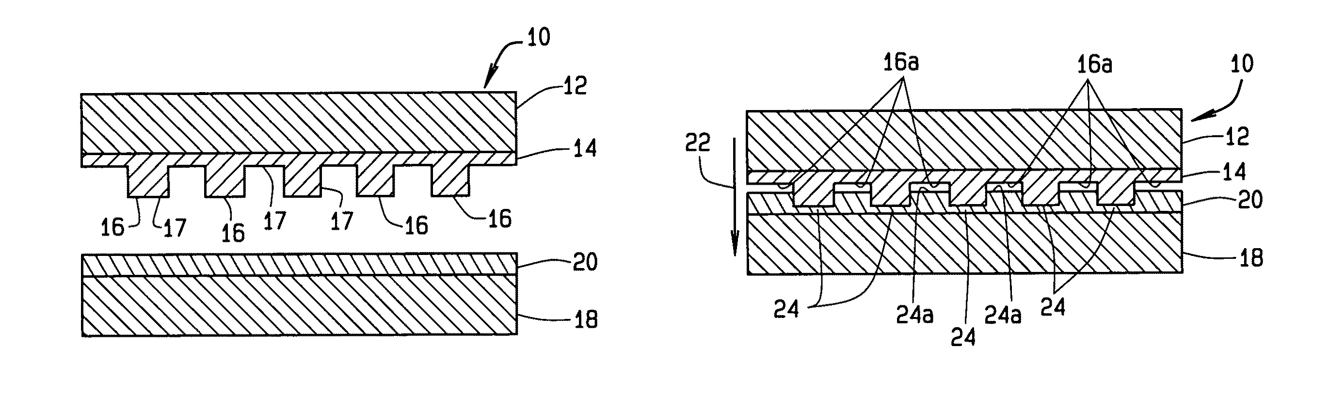
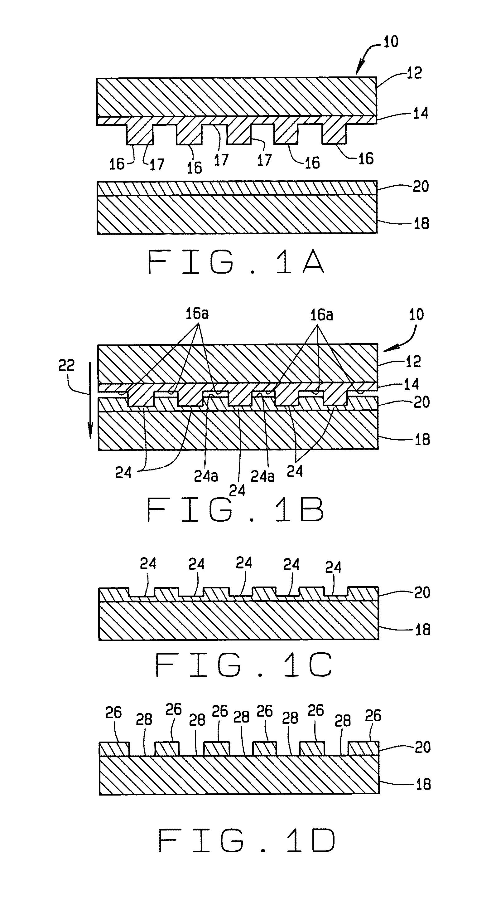
[0031]This invention also relates to a method and apparatus for a resolution, high-throughput, lithography. Unlike current microlithography, a preferred embodiment of the present invention abandons usage of energetic light or particle beams. The present invention is based on pressing a mold into a thin film on a substrate to create a relief and, later removing the compressed area of the film to expose the underlying substrate and to form a resist pattern on the substrate that replicates the obverse of the protruding pattern of the mold.

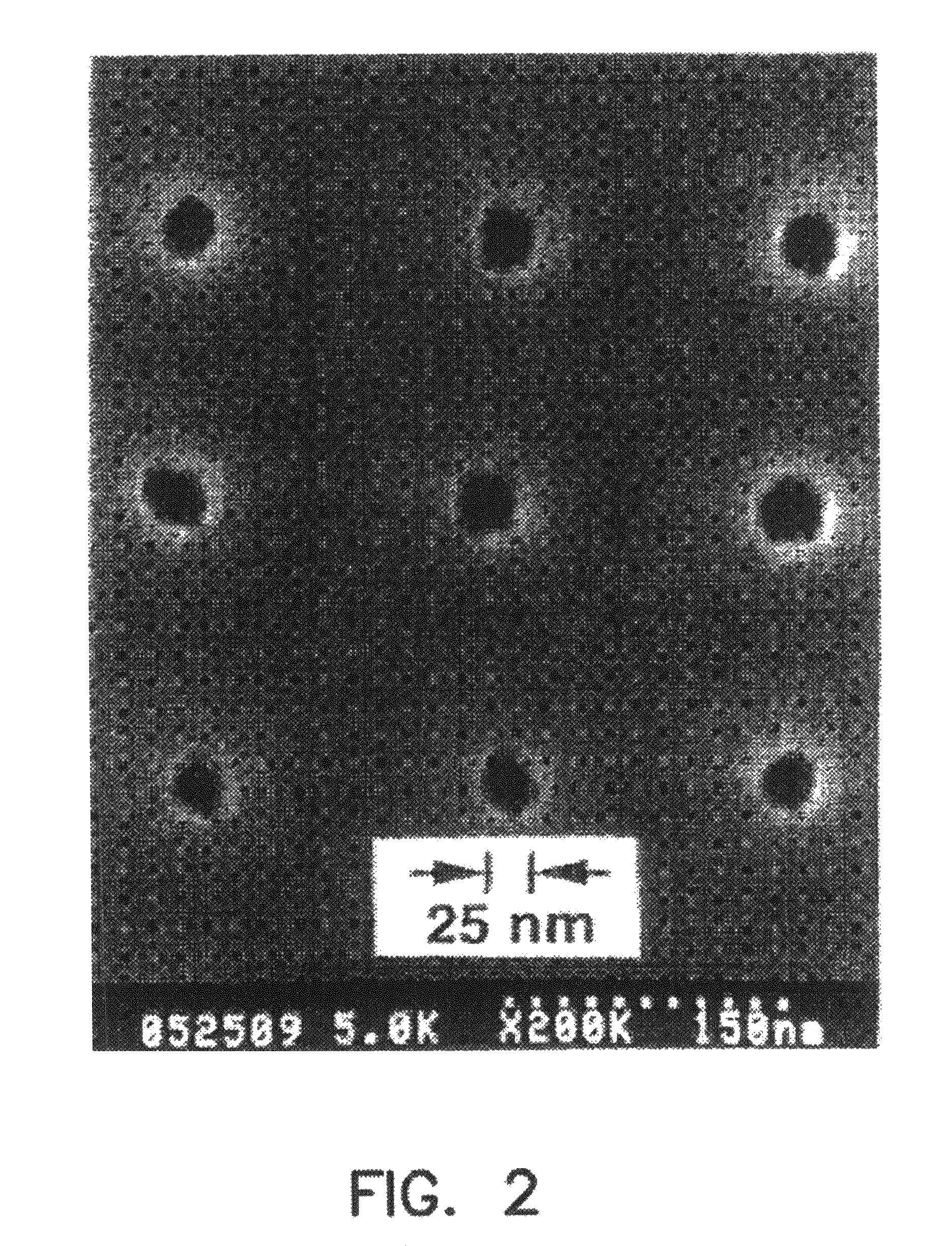
[0032]The present invention also has demonstrated the generation of patterns, such as holes, pillars, or trenches in a thin film on a substrate, that have a minimum size of 25 nm, a depth over 100 nm, a side wall smoothness better than 3 nm, and corners with near perfect 90 degrees angles. it was found that presently the size of imprinted features is limited by the size of the mold being used; with a suitable mold, the present invention should create ...


PUM

PropertyMeasurementUnit
depthaaaaaaaaaa
sizesaaaaaaaaaa
sizeaaaaaaaaaa

Abstract

A method to forming a pattern on a surface of a substrate, including the steps of providing a mold having a molding surface comprised of one or more protruding features and one or more recessed features for imprinting a pattern. The pattern comprising at least one feature having a lateral dimension of about 2000 nanometer or less. Providing a monomolecular anti-adhesive layer on the mold which is either continuous or discontinuous, prior to depositing a hardenable, flowable material onto the mold and recessed features. The mold and substrate are pressed together, while the flowable material hardens and adheres to the moldable material and the substrate. Upon separation of the mold and the substrate, the hardened material remains on the substrate.

Description

CROSS-REFERENCE TO RELATED APPLICATIONS[0001]The present application is a continuation-in-part of U.S. patent application Ser. No. 11 / 003,107 by Stephen Y. Chou, filed on Dec. 3, 2004, from which priority is claimed and which is herein incorporated by reference. The '107 application is a divisional of U.S. patent application Ser. No. 10 / 244,303, filed Sep. 16, 2002, which is a continuation of U.S. patent application Ser. No. 10 / 046,594, filed on Oct. 29, 2001, which is a divisional of U.S. patent application Ser. No. 09 / 107,006 filed on Jun. 30, 1998, now U.S. Pat. No. 6,309,580, which is a continuation-in-part of U.S. patent application Ser. No. 08 / 558,809, filed on Nov. 15, 1995, now U.S. Pat. No. 5,772,905. Each of the aforementioned patents and applications is herein incorporated by reference.[0002]The present application is related to U.S. patent application Ser. No. 10 / 244,276 filed by Stephen Y. Chou on Sep. 16, 2002 and entitled “Lithographic Method For Molding Pattern With ...

Claims


Application Information

Patent Timeline
Patent Type & Authority Patents(United States)
IPC IPC(8): B29C33/64
CPCB29C33/60B29C33/64B29C37/0053B29C59/022B82Y10/00B82Y40/00G03F7/0002B29C2059/023
Inventor CHOU, STEPHEN Y.
Owner RGT UNIV OF MINNESOTA
Why Eureka
Try Eureka