Semiconductor die with integrated electro-static discharge device

a technology of electro-static discharge device and semiconductor body, which is applied in the direction of circuit arrangement, emergency protective circuit arrangement, etc., can solve the problems of significant damage to the integrated circuit, significant increase in parasitic capacitance of input/output pads, and problem of increasing parasitic capacitance, etc., to achieve the effect of reducing the capacitan

a technology of electro-static discharge device and semiconductor body, which is applied in the direction of circuit arrangement, emergency protective circuit arrangement, etc., can solve the problems of significant damage to the integrated circuit, significant increase in parasitic capacitance of input/output pads, and problem of increasing parasitic capacitance, etc., to achieve the effect of reducing the capacitan

US8183593B2Active Publication Date: 2012-05-22ORACLE INT CORP

Image

  • Semiconductor die with integrated electro-static discharge device
  • Semiconductor die with integrated electro-static discharge device
  • Semiconductor die with integrated electro-static discharge device

Examples


Embodiment Construction

[0031]The following description is presented to enable any person skilled in the art to make and use the disclosure, and is provided in the context of a particular application and its requirements. Various modifications to the disclosed embodiments will be readily apparent to those skilled in the art, and the general principles defined herein may be applied to other embodiments and applications without departing from the spirit and scope of the present disclosure. Thus, the present disclosure is not intended to be limited to the embodiments shown, but is to be accorded the widest scope consistent with the principles and features disclosed herein.

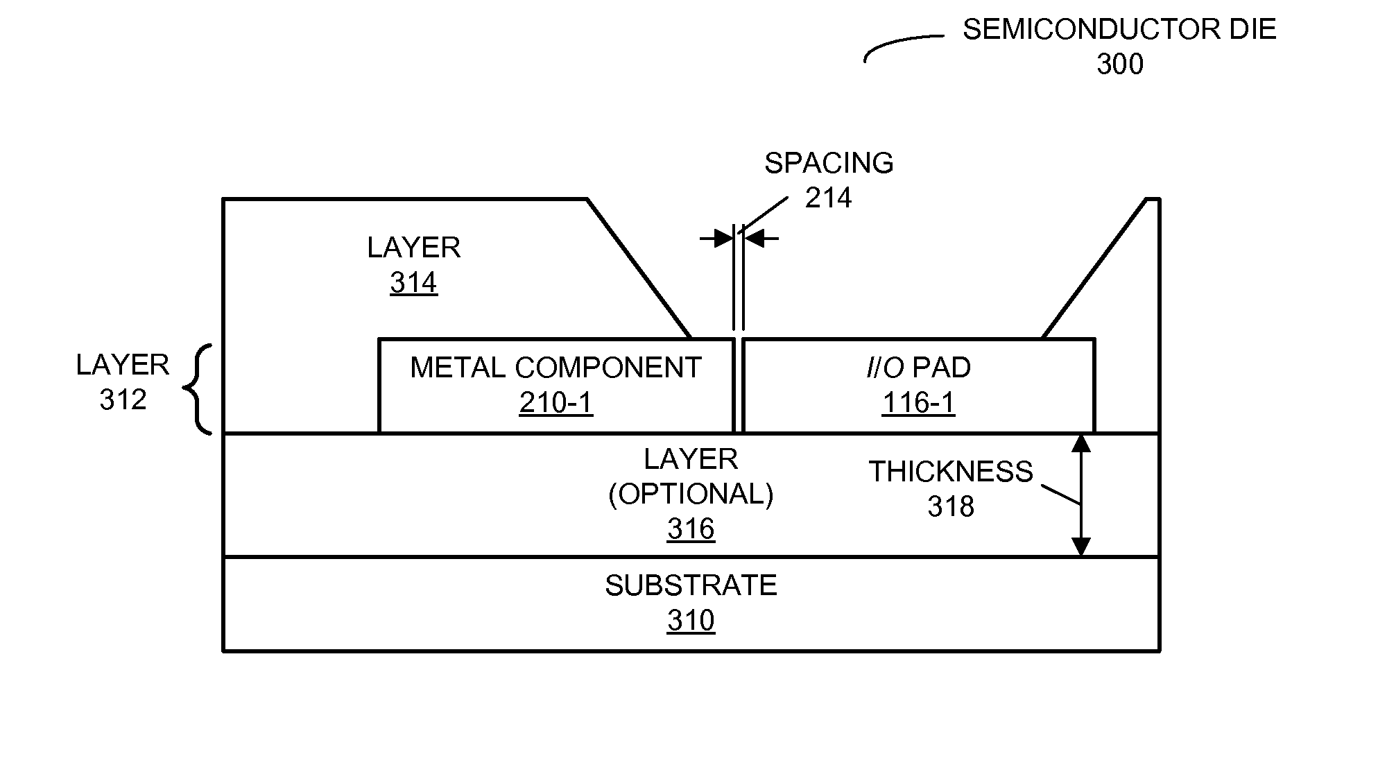
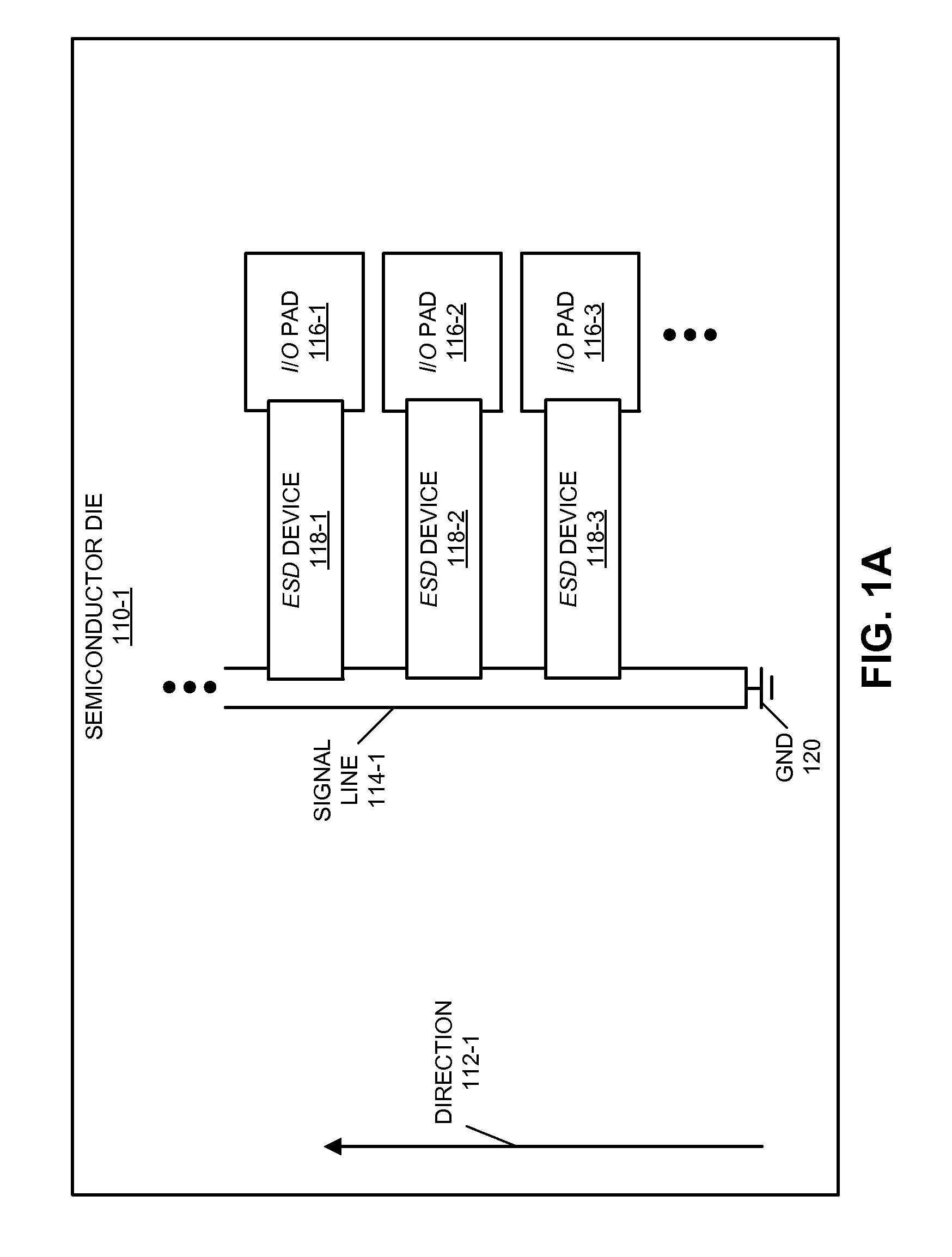
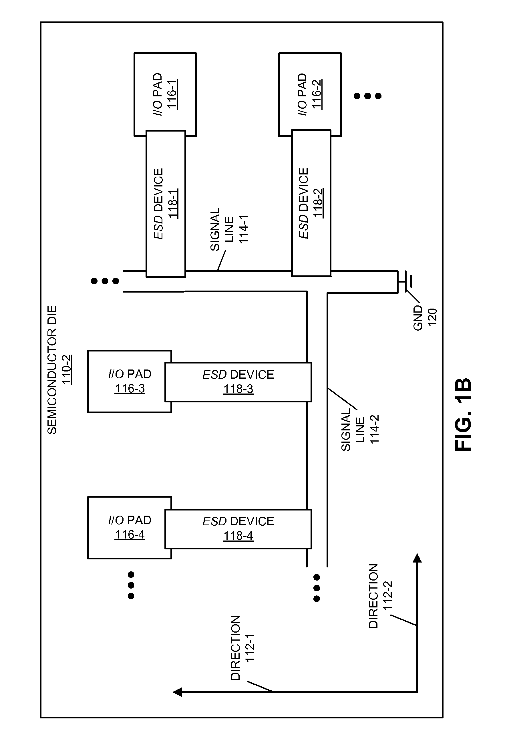
[0032]Embodiments of a semiconductor die, a chip package that includes the semiconductor die, and an electronic device that includes the chip package are described. This semiconductor die includes an ESD device with a metal component coupled to an I / O pad, and coupled to ground via a signal line. Moreover, adjacent edges of the metal compone...


PUM


Abstract

A semiconductor die is described. This semiconductor die includes an electro-static discharge (ESD) device with a metal component coupled to an input-output (I / O) pad, and coupled to a ground voltage via a signal line. Moreover, adjacent edges of the metal component and the I / O pad are separated by a spacing that defines an ESD gap. When a field-emission or ionization current flows across the ESD gap, the metal component provides a discharge path to the ground voltage for transient ESD signals. Furthermore, the ESD gap is at least partially enclosed so that there is gas in the ESD gap.

Description

BACKGROUND[0001]1. Field[0002]The present disclosure relates to a semiconductor die that includes an integrated electro-static discharge (ESD) device to protect the semiconductor die from transient ESD signals.[0003]2. Related Art[0004]ESD events commonly arise during the manufacture, assembly or use of systems containing integrated circuits. While the amount of energy dissipated during an ESD event may be comparatively small on a human scale (akin to the shock you receive when touching a metal object after walking across a thick carpet), from the perspective of the small, sensitive electronics on an integrated circuit, the destructive power can be comparable to a lightning strike, and can cause significant damage to integrated circuits.[0005]A variety of existing ESD-protection circuits and techniques are used to protect integrated circuits from ESD events. For example, one existing ESD-protection circuit includes reverse-biased metal-oxide-semiconductor (MOS) or PN diodes that tur...

Claims


Application Information

Patent Timeline
22 May 2012
Publication
US8183593B2
IPC
H01L29/72; H01L23/552; H01L31/111; H01L29/73; H01L29/74; H01L23/62
CPC
H01L23/60; H01L27/0288; H01L2924/0002; H01L2924/00014; H01L2924/1305; H01L2924/13091; H01L2224/02166; H01L2224/05567
Inventors
DROST, ROBERT J.; HOPKINS, ROBERT D.