Input device

a technology of input device and input device, which is applied in the direction of static indicating device, instruments, contacts, etc., to achieve the effect of high resolution

Inactive Publication Date: 2012-07-03
PANASONIC CORP
View PDF14 Cites 3 Cited by
  • Summary
  • Abstract
  • Description
  • Claims
  • Application Information

AI Technical Summary

Benefits of technology

[0011]The present invention addresses the conventional problems, and provides an input device that has a circular arc resistive layer, has no failure during operation at an angle position between the ends of the circular arc resistive layer, can detect an operation position, and has high resolution.
[0013]Therefore, an input device can be achieved inexpensively where the operation-position detection state and power consumption state during operation between both ends of the circular arc resistive layer or at an angle position near each of the ends are equivalent to those at other angle positions, the operation position can be detected over the full circumference, and the resolution is high.

Problems solved by technology

However, the conventional input device has the following problem: when operation body 15 is tilted in an angle direction between ends 1A and 1B of circular arc resistive layer 1, ends 1A and 1B simultaneously come into contact with conductive layer 3 to provide a substantial short-circuit state.
In this state, the quantity of flowing current increases to hasten the battery consumption, the output of the partial voltage ratio is the same as the output at the diagonal position to disable determination of the operation position, disadvantageously.

Method used


Image

  • Input device
  • Input device
  • Input device

Examples


first exemplary embodiment

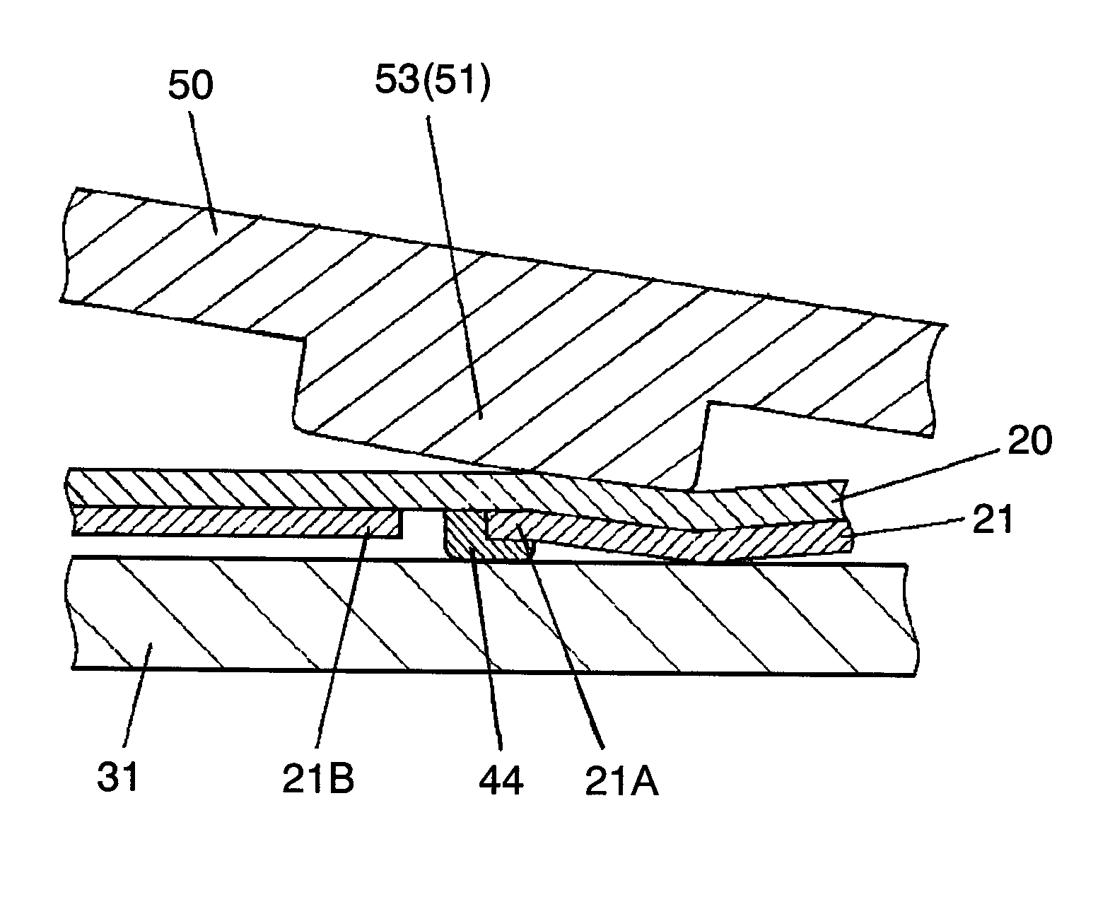
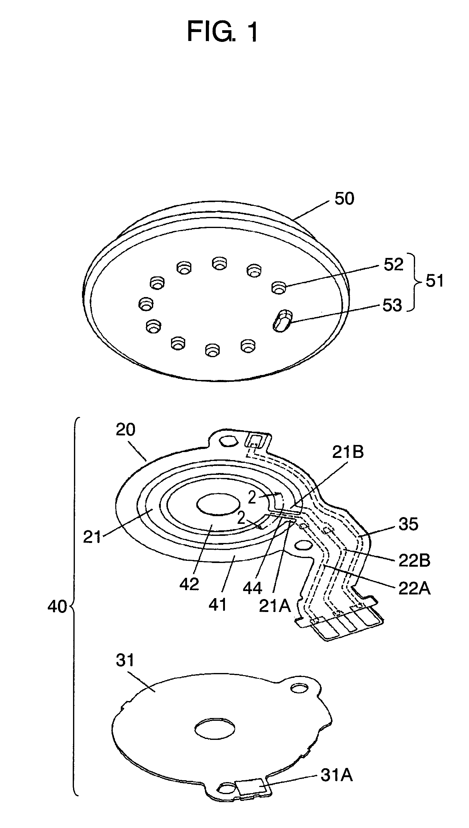
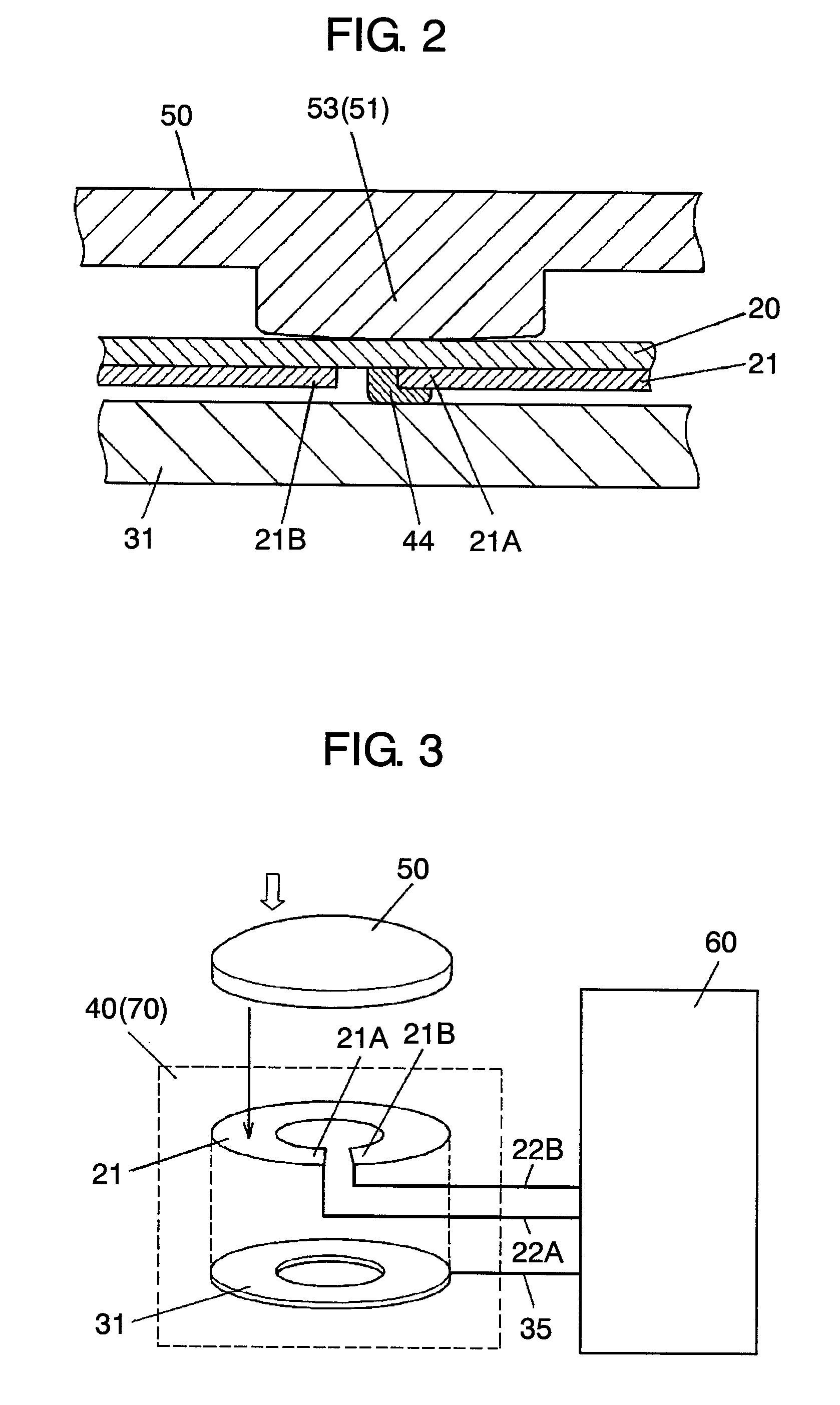
[0026]FIG. 1 is an exploded perspective view of element unit 40 of an input device in accordance with exemplary embodiment 1 of the present invention. FIG. 2 is a partial sectional view of element unit 40 of the input device that is taken in the broken line pointed by arrows 2 of FIG. 1. FIG. 3 is a conceptual diagram of the input device in accordance with exemplary embodiment 1.

[0027]In FIG. 1, element unit 40 of the input device has substrate 20 and metal plate 31. Substrate 20 is a flexible resin film made of polyethylene terephthalate (PET) or the like, is formed in a shape having a tail part, and has circular arc resistive layer 21 printed on its lower face. Circular arc resistive layer 21 has a constant radial width. Ends 21A and 21B on both sides of circular arc resistive layer 21 are coupled to one-end sides of independent conductive first patterns 22A and 22B formed on the lower face of substrate 20, respectively. The-other-end sides of first patterns 22A and 22B are couple...

second exemplary embodiment

[0054]FIG. 6 is an exploded perspective view of element unit 70 of an input device in accordance with exemplary embodiment 2 of the present invention. FIG. 7 is a partial sectional view of element unit 70 of the input device that is taken in the broken line pointed by arrows 7 of FIG. 6. Element unit 70 of the input device of exemplary embodiment 2 has an insulating film used as a contact preventing unit at a position different from that in exemplary embodiment 1. However, the other elements have much the same structure as that of exemplary embodiment 1, so that the same elements are denoted with the same reference marks and are not described in detailed.

[0055]Element unit 70 of the input device of embodiment 2 has the following structure shown in FIG. 6, similarly to element unit 40 of the input device of embodiment 1. Circular arc resistive layer 21 formed on the lower face of substrate 20 is vertically faced to metal plate 31 as a conductive layer at a predetermined distance. Fir...


PUM

PropertyMeasurementUnit
angleaaaaaaaaaa
angleaaaaaaaaaa
conductiveaaaaaaaaaa

Abstract

An input device has a circular arc resistive layer and a metal plate as a conductive layer that is faced to the circular arc resistive layer, and can detect a position operated by partial contact between them. The input device has an element unit where a linear insulating layer as a contact preventing unit for preventing both ends of the circular arc resistive layer from simultaneously coming into contact with the metal plate during operation is disposed on one end of the circular arc resistive layer.

Description

BACKGROUND OF THE INVENTION[0001]1. Field of the Invention[0002]The present invention relates to an input device constituting an operation unit of various electronic apparatuses.[0003]2. Background Art[0004]Recently, various electronic apparatuses have been miniaturized and lightened in weight. The number of electronic apparatuses operated by selecting a predetermined function by moving a cursor displayed on a screen have been increased. A conventional input device corresponding to the operation form of the various electronic apparatuses is described hereinafter with reference to the drawings.[0005]FIG. 9 is a conceptual diagram of a conventional input device. In FIG. 9, element unit 10 of the conventional input device includes circular arc resistive layer 1 and a circular-ring-like conductive layer 3 facing circular arc resistive layer 1 at a predetermined distance. Each of ends 1A and 1B of circular arc resistive layer 1 and conductive layer 3 are coupled to control unit 5. Circul...

Claims


Application Information

Patent Timeline
Patent Type & Authority Patents(United States)
IPC IPC(8): G09G5/00H01C10/06G08C19/12H01H19/00G06F3/0338
CPCG06F3/0338H01H25/041H01H2201/036H01H2239/078H01H13/704H01H13/00
Inventor SAWADA, MASAKIYAMAMOTO, TAMOTSUINOUE, HIROTO
Owner PANASONIC CORP
Why Eureka
Try Eureka