Turning off buffer when a digital back end operates at a same data rate as the analog front end

a digital back end and data rate technology, applied in the field of signal processors, can solve the problems of reducing the amount by which the supply voltage can be reduced, the primary source of power consumption of the circuit, and the use of expensive voltage regulators, so as to reduce the leakage power of the processor without significantly affecting performance and/or area, and save power

Inactive Publication Date: 2012-08-21
AVAGO TECH WIRELESS IP SINGAPORE PTE
View PDF14 Cites 0 Cited by
  • Summary
  • Abstract
  • Description
  • Claims
  • Application Information

AI Technical Summary

Benefits of technology

[0005]Illustrative embodiments of the present invention meet the above-noted need by presenting techniques for beneficially reducing leakage power in a processor without significantly impacting performance and / or area. To accomplish this, embodiments of the invention provide a processor including an analog front end, a digital back end, and a buffer connected between the analog front end and digital back end. The digital back end is allowed to operate at the highest data rate of the analog front end. When the analog front end is operating at a lower data rate than the digital back end, data generated by the analog front end is stored in the buffer. While the buffer is filling, the digital back end is turned off to conserve power. When the buffer is full, the digital back end is turned on and data stored in the buffer is read at the higher data rate until the buffer is empty (or at least no longer full), at which point the digital back end is turned off again and the process is repeated. Since the digital back end is turned off for at least a portion of the time that data is being stored in the buffer, leakage power in the processor is advantageously reduced.
[0007]In accordance with another aspect of the invention, a method for reducing power consumption in a processor including an analog front end and a digital back end includes the steps of: detecting a data rate of the analog front end relative to a data rate of the digital back end; storing data associated with an output of the analog front end in a buffer in a first mode of operation corresponding to when the data rate of the analog front end is less than the data rate of the digital back end; and bypassing the buffer in a second mode of operation corresponding to when the data rate of the analog front end is substantially equal to the data rate of the digital back end.

Problems solved by technology

In many data processing circuits, the DSP is a primary source of power consumption in the circuits.
However, operating the DSP at a lower supply voltage has several disadvantages.
For example, operating the DSP at a lower supply voltage for lower data rates requires the use of expensive voltage regulators.
Furthermore, the amount by which the supply voltage can be reduced is limited by worst case transistor threshold voltage levels in the circuit (e.g., about 0.85 volt, depending on the integrated circuit process technology) and the amount of overdrive required in the circuit (the term “overdrive” generally refers to the level of gate voltage above the threshold voltage required for a given transistor device).

Method used


Image

  • Turning off buffer when a digital back end operates at a same data rate as the analog front end
  • Turning off buffer when a digital back end operates at a same data rate as the analog front end
  • Turning off buffer when a digital back end operates at a same data rate as the analog front end

Examples


Embodiment Construction

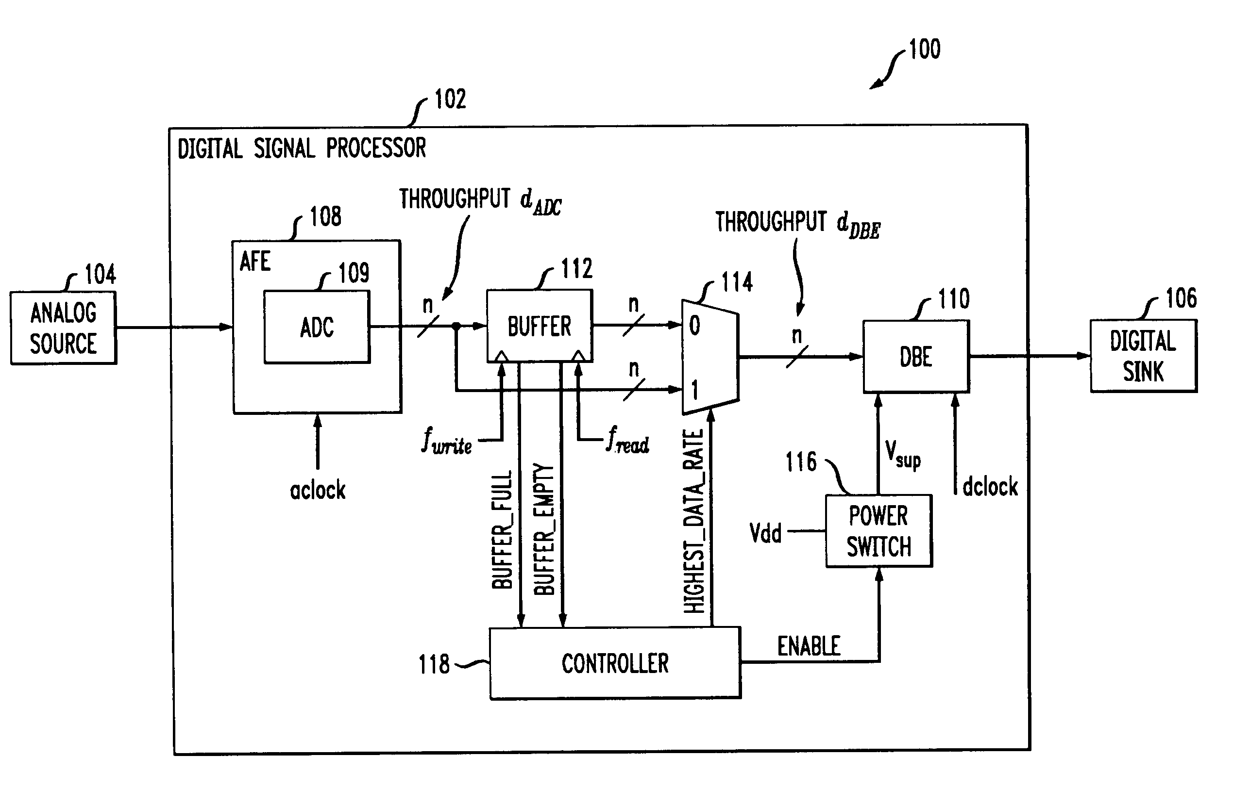
[0012]The present invention will be described herein in the context of an exemplary processor circuit, such as a DSP circuit, and an illustrative buffer circuit for use therein. It is to be understood, however, that the techniques of the present invention are not limited to the circuits shown and described herein. Rather, embodiments of the invention are directed to techniques for reducing power consumption in a processor circuit, without significantly impacting performance and / or area of the circuit. Although preferred embodiments of the invention may be fabricated in a silicon wafer, embodiments of the invention can alternatively be fabricated in wafers comprising other materials, including but not limited to gallium arsenide (GaAs), indium phosphide (InP), etc.

[0013]With reference to FIG. 1, a block diagram depicts at least a portion of an exemplary signal processing system 100 having reduced power consumption, in accordance with an embodiment of the present invention. The signal...


PUM


Abstract

A processor circuit having reduced power consumption includes an analog front end operative to receive an analog signal supplied to the processor circuit and to generate a digital signal indicative of the analog signal. The processor further includes a digital back end operative to generate a digital output signal as a function of the digital signal generated by the analog front end. A buffer is coupled between the analog front end and the digital back end. In a first mode of operation, the digital back end operates at a substantially same data rate as the analog front end and the buffer is bypassed. In a second mode of operation, the digital back end operates at a higher data rate than the analog front end and the buffer is used to store outputs of the analog front end.

Description

FIELD OF THE INVENTION[0001]The present invention relates generally to the electrical and electronic arts, and more particularly relates to signal processors.BACKGROUND OF THE INVENTION[0002]The use of signal processors, such as, for example, digital signal processors (DSPs), for supporting multiple data rates in certain applications is well known. Such applications may include, for example, read channels for hard disk drives supporting a wide range of data rates because the disk spins at a constant angular velocity, read channels for optical storage supporting multiple data rates (e.g., 1×, 2×, 4×, 8× read speeds), and Ethernet or wireless local area network (LAN) transceivers supporting multiple data rates (e.g., 10 / 100 / 1000 / 10000 megabits per second (Mb / s) for Gigabit Ethernet).[0003]In many data processing circuits, the DSP is a primary source of power consumption in the circuits. For certain applications, particularly portable applications, reducing power consumption is critica...

Claims


Application Information

Patent Timeline
Patent Type & Authority Patents(United States)
IPC IPC(8): G06F1/32G06F13/00G06F3/00
CPCG06F1/3287G11B20/10037G11B20/10527G06F1/3221Y02B60/1246G11B2020/10759G11B2220/2516Y02B60/1282Y02D10/00G06F1/3203G06F1/32G06F9/00
Inventor GRAEF, NILS
Owner AVAGO TECH WIRELESS IP SINGAPORE PTE
Why Eureka
Try Eureka