Method and structure for forming relatively dense conductive layers

a technology of conductive layer and conductive layer, which is applied in the direction of semiconductor/solid-state device details, semiconductor devices, electrical devices, etc., can solve the problems of increasing susceptibility to manufacturing defects and general performance degradation of the integrated circuit, and achieve the effect of reducing manufacturing defects

Active Publication Date: 2008-05-20
SILICON LAB INC
View PDF37 Cites 2 Cited by
  • Summary
  • Abstract
  • Description
  • Claims
  • Application Information

AI Technical Summary

Benefits of technology

[0005]A high metal density region may be placed in metal layers proximate to an area of low metal density extending from an inductor through multiple integrated circuit layers without violating manufacturing design rules for reducing manufacturing defects and without substantially impacting performance of the inductor. These results are achieved by including a transitional region between the region of high metal density and the region of low metal density. The transitional region has a structure that allows at most a negligible amount of current flow to be induced in the structure.

Problems solved by technology

An inductor formed on an integrated circuit is generally susceptible to performance degradation due to electromagnetic coupling of conductive structures near the inductor.
Unfortunately, in some integrated circuit manufacturing processes, areas of high metal density adjacent to areas of low metal density, in the same or even different metal layers, may have increased susceptibility to manufacturing defects and violate design rules implemented to reduce the impact of these defects in the particular process.

Method used


Image

  • Method and structure for forming relatively dense conductive layers
  • Method and structure for forming relatively dense conductive layers
  • Method and structure for forming relatively dense conductive layers

Examples


Embodiment Construction

)

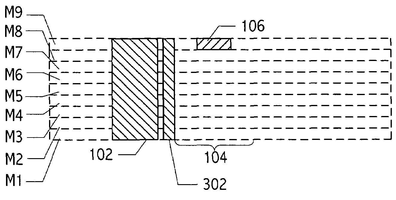
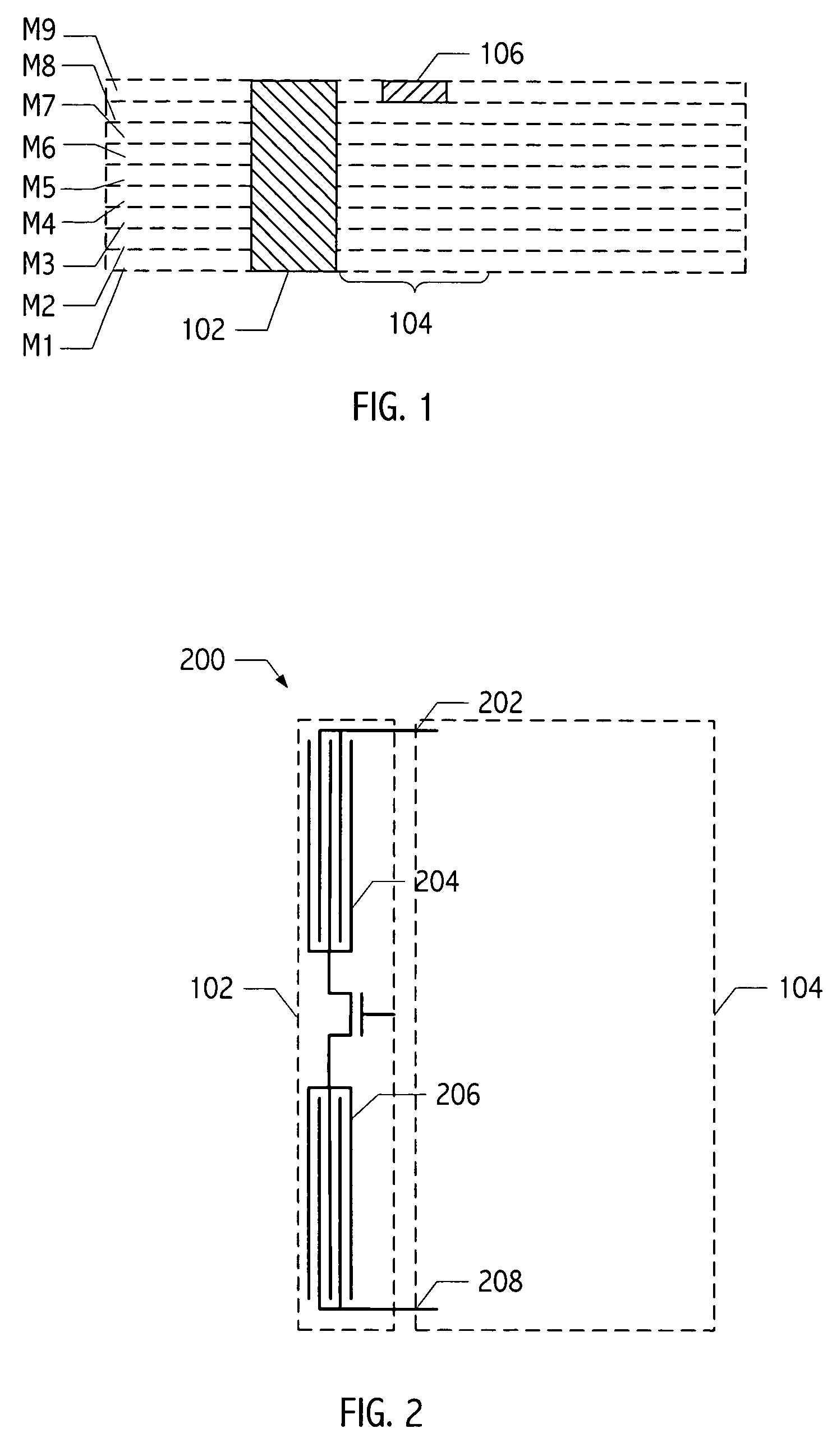
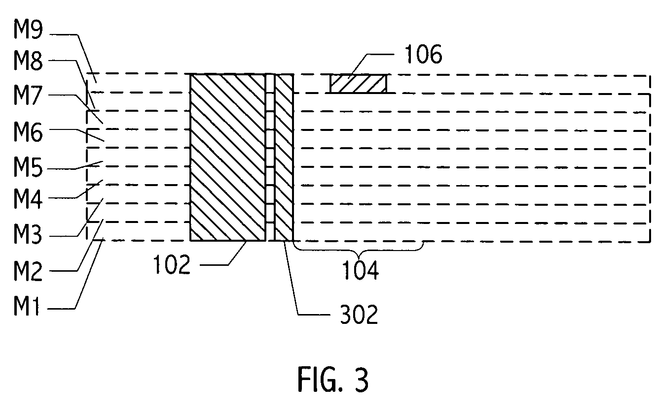
[0017]Referring to FIG. 1, an exemplary inductor (e.g., inductor 106) and a region of high conductor density (e.g., region 102), are formed in a typical integrated circuit manufacturing process. A region of high conductor density is a region including conductive structures. For example, an integrated circuit manufacturing process may require that conductive layers have a conductor density ranging from 20 to 80%. The density requirements will depend upon a particular manufacturing process. Typical conductors are formed of metals such as copper or aluminum. A volume of space beneath inductor 106, e.g., region 104, is void of conductive structures, i.e., the space is a region of low metal density included to prevent the electromagnetic field of the inductor from inducing a current in a metal structure that generates an electromagnetic field that counteracts the field of the inductor.

[0018]One structure that may be formed in high density metal region is a capacitor shown in FIG. 2. Typ...


PUM

PropertyMeasurementUnit
densityaaaaaaaaaa
conductiveaaaaaaaaaa
impedanceaaaaaaaaaa

Abstract

A region of high metal density may be placed in metal layers proximate to an area of low metal density below an inductor on an integrated circuit without violating manufacturing design rules for reducing manufacturing defects and without substantially impacting performance of the inductor. These results are achieved by including a transitional region that includes conductive structures electrically isolated from each other between the region of high metal density and the region of low metal density. The transitional region has a structure that allows a negligible amount of current flow to be induced in the structure.

Description

CROSS-REFERENCE TO RELATED APPLICATION(S)BACKGROUND[0001]1. Field of the Invention The present invention relates to integrated circuits, and more particularly to such integrated circuits incorporating inductors.[0002]2. Description of the Related Art[0003]An inductor formed on an integrated circuit is generally susceptible to performance degradation due to electromagnetic coupling of conductive structures near the inductor. In designs particularly sensitive to inductor performance, the impact of the coupling from these electromagnetic signals may be lessened by reducing or eliminating structures that affect performance. Accordingly, a design may reduce or eliminate conductive structures near an inductor, generating areas of the integrated circuit having a low metal density extending from the inductor through one or more integrated circuit layers. Unfortunately, in some integrated circuit manufacturing processes, areas of high metal density adjacent to areas of low metal density, in ...

Claims


Application Information

Patent Timeline
Patent Type & Authority Patents(United States)
IPC IPC(8): H01L23/52H01L21/8222H01L23/522H01L27/08
CPCH01L23/5223H01L23/5227H01L27/08H01L2924/3011H01L2924/0002H01L2924/00
Inventor ZHANG, LIGANG
Owner SILICON LAB INC
Why Eureka
Try Eureka