Memory built-in self-characterization

a memory and self-characterization technology, applied in the field of memory circuits, can solve the problems of significantly increasing the total power consumption of the ic, exhibiting higher active and leakage and significantly increasing the percentage of total power consumption in the ic attributable to memory circuits, so as to reduce the power consumption in the ic without significantly affecting the performance of the ic, and minimize power consumption

Active Publication Date: 2012-05-01
LSI CORP
View PDF17 Cites 4 Cited by
  • Summary
  • Abstract
  • Description
  • Claims
  • Application Information

AI Technical Summary

Benefits of technology

[0006]Illustrative embodiments of the present invention provide techniques for reducing power consumption in an IC without significantly impacting performance of the IC. To accomplish this, embodiments of the invention advantageously control a level of voltage supplied to one or more memory circuits in the IC to achieve a prescribed operation of the memory circuits while minimizing power consumption and limiting leakage current in the memory circuit to a prescribed level.
[0008]In accordance with another aspect of the invention, a method of operating a circuit including an operational memory so as to reduce overall power consumption in the circuit includes the steps of: measuring at least one functional characteristic of the operational memory using a monitor circuit, the monitor circuit comprising a circuit element in the operational memory and / or a circuit element substantially identical to a corresponding circuit element in the operational memory; generating a control signal which varies as a function of the at least one functional characteristic of the operational memory; and controlling a level of at least one of a voltage and a current supplied to at least a portion of the operational memory as a function of the control signal.

Problems solved by technology

Unfortunately, these two objectives have significantly increased the total power consumption in the IC.
Moreover, the percentage of total power consumption in the IC attributable to memory circuits has increased dramatically.
Memory circuits are operated at greater speeds with higher applied voltage, and therefore exhibit higher active and leakage power consumption in an IC.
For example, a fast IC process typically produces transistors and other circuit elements which tend to operate at relatively fast speeds but which consume relatively high power compared to a normal IC fabrication process.
Alternatively, a slow IC process typically produces transistors and other circuit elements that tend to consume relatively low power but operate at relatively slow speeds compared to a normal IC fabrication process.
Temperature also affects memory speed and power consumption in the IC, primarily due to leakage current.
However, such conventional process monitors directed to the general IC are not capable of adequately measuring operational performance within the memory circuits.
Consequently, techniques for optimizing power consumption in the memory circuits, which contribute to an ever-increasing percentage of the overall IC power consumption, are ineffective.

Method used


Image

  • Memory built-in self-characterization
  • Memory built-in self-characterization
  • Memory built-in self-characterization

Examples


Embodiment Construction

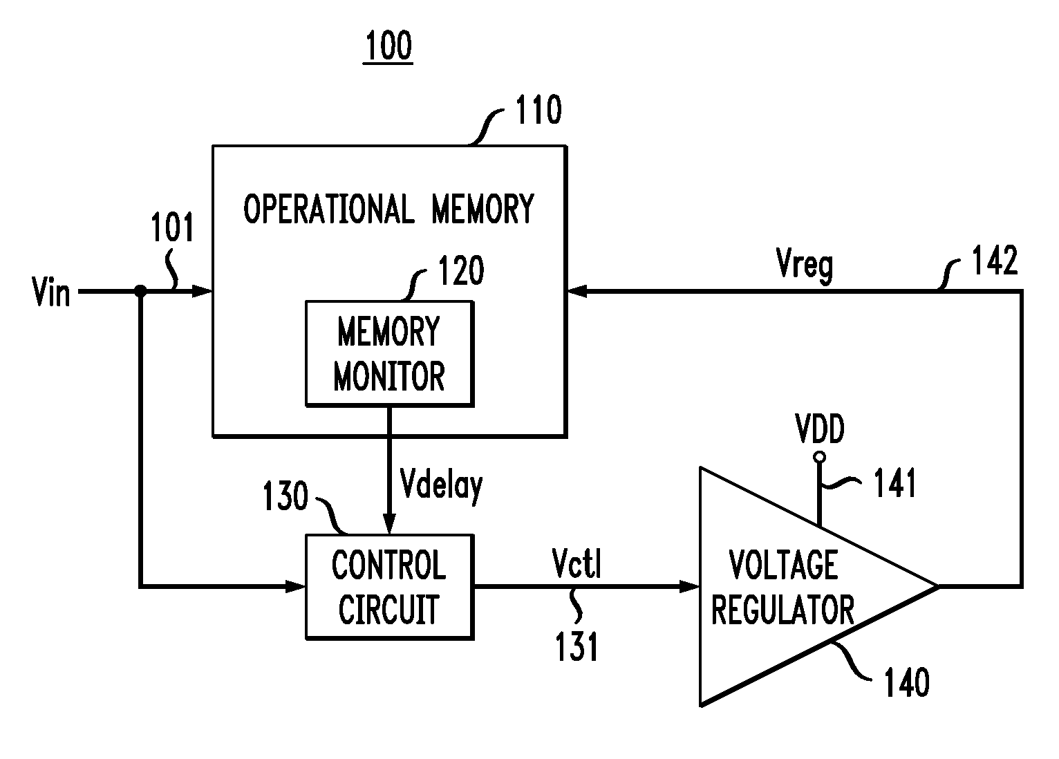
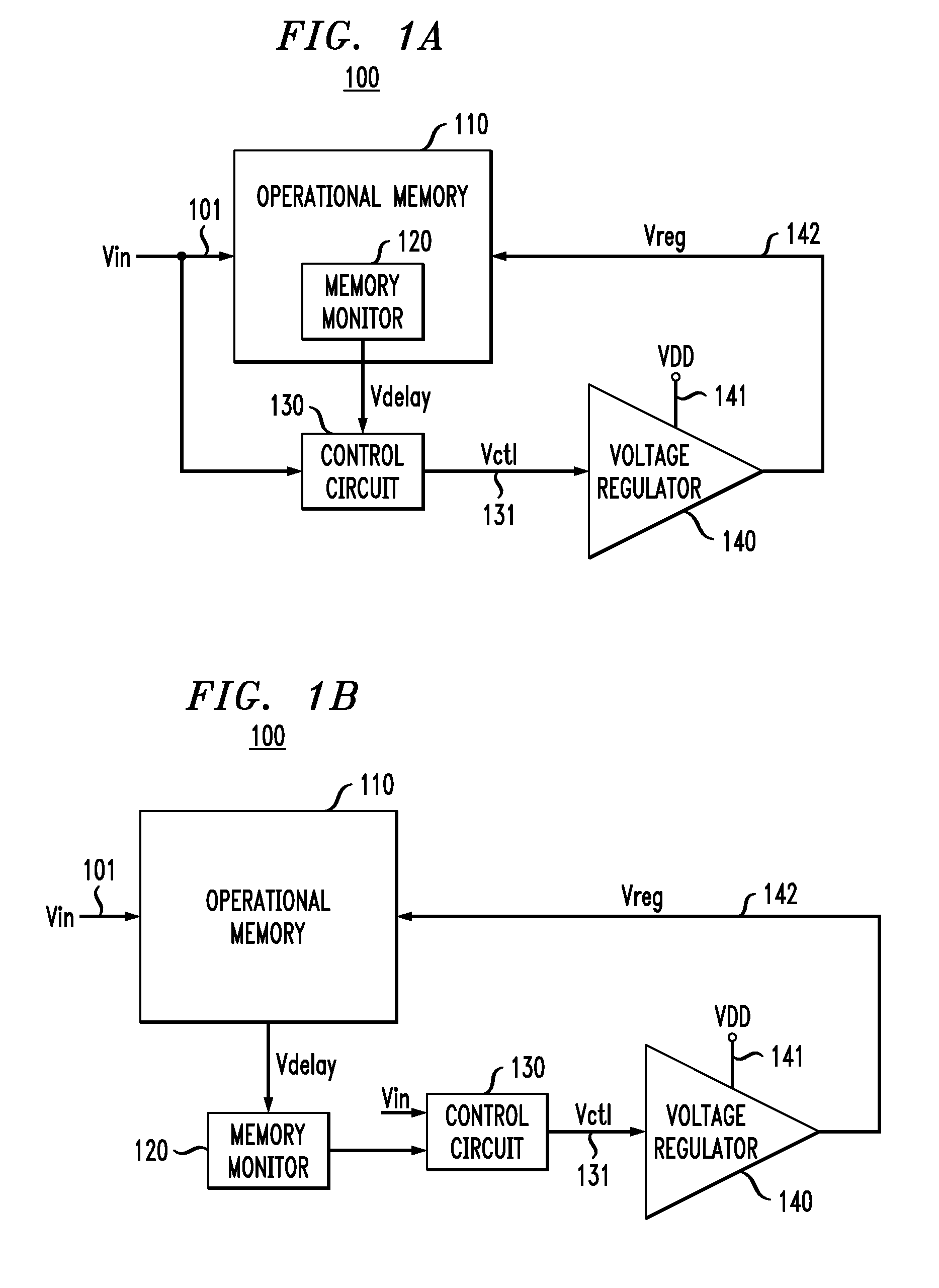
[0020]The present invention will be described herein in the context of illustrative memory circuits and a method for reducing power consumption in a memory circuit. It is to be appreciated, however, that the techniques of the present invention are not limited to the specific method and circuits shown and described herein. Rather, embodiments of the invention are directed broadly to techniques for beneficially reducing power consumption in a memory circuit without significantly impacting performance of the memory circuit. For this reason, numerous modifications can be made to these embodiments and the results will still be within the scope of the invention. No limitations with respect to the specific embodiments described herein are intended or should be inferred.

[0021]Although implementations of the present invention may be described herein with specific reference to n-channel metal-oxide-semiconductor (NMOS) transistors devices and p-channel metal-oxide-semiconductor (PMOS) transis...


PUM


Abstract

A memory circuit includes an operational memory and a monitor circuit comprising a circuit element in the operational memory and / or a circuit element substantially identical to a corresponding circuit element in the operational memory. The monitor circuit is operative to measure at least one functional characteristic of the operational memory. A control circuit coupled to the monitor circuit is operative to generate a control signal which varies as a function of the measured characteristic of the operational memory. The memory circuit further includes a programmable voltage source coupled to the operational memory which is operative to generate at least a voltage and / or a current supplied to at least a portion of the operational memory which varies as a function of the control signal.

Description

FIELD OF THE INVENTION[0001]The present invention relates generally to the electrical, electronic, and computer arts, and more particularly relates to memory circuits.BACKGROUND OF THE INVENTION[0002]A trend in modern integrated circuits (ICs) is to include more and larger memory circuits on chip (e.g., embedded memory) for performing various functions of the IC. There is also a trend to shrink geometries (e.g., feature sizes) of circuit elements in the IC to thereby increase the number of functions incorporated into the IC and / or to reduce die size, and thereby reduce manufacturing cost. Unfortunately, these two objectives have significantly increased the total power consumption in the IC. Moreover, the percentage of total power consumption in the IC attributable to memory circuits has increased dramatically.[0003]Memory circuits are operated at greater speeds with higher applied voltage, and therefore exhibit higher active and leakage power consumption in an IC. IC manufacturing p...

Claims


Application Information

Patent Timeline
Patent Type & Authority Patents(United States)
IPC IPC(8): G11C7/00
CPCG11C5/147G11C11/417
Inventor AZIMI, KOUROSFRATTI, ROGER A.GEORGE, DANNY MARTINMCPARTLAND, RICHARD J.
Owner LSI CORP
Why Eureka
Try Eureka