

Semiconductor layout modification method based on design rule and user constraints
- Summary
- Abstract
- Description
- Claims
- Application Information
AI Technical Summary
Benefits of technology
Problems solved by technology
Method used
Image

Examples
Embodiment Construction
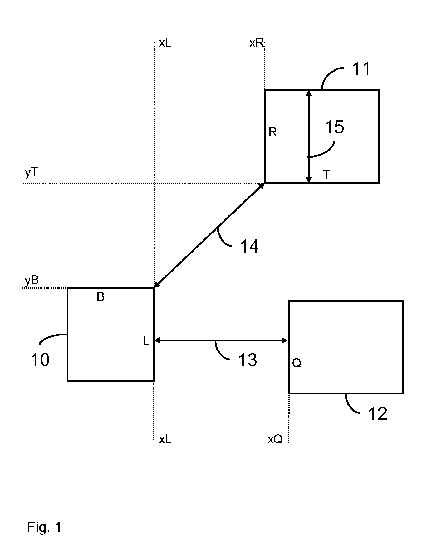
[0025]FIG. 1 shows a part of a 2-D semiconductor layout with three objects (10, 11, 12). Depending on their function, the objects (10, 11, 12) may be of conducting, semi-conducting or insulating material. The layout may, e.g., comprise transistors, wires, resistors, capacitors and the like. In FIG. 1, the objects are represented as polygons. In accordance with the method described in the European patent application No. 07104863, the topology of the layout is stored in a database with edges and proximities. Proximities (13, 14, 15) are relations between edges or corners that are direct neighbors. FIG. 1 shows part of the proximity relations (13, 14, 15) between edges and corners of the shown objects (10, 11, 12).
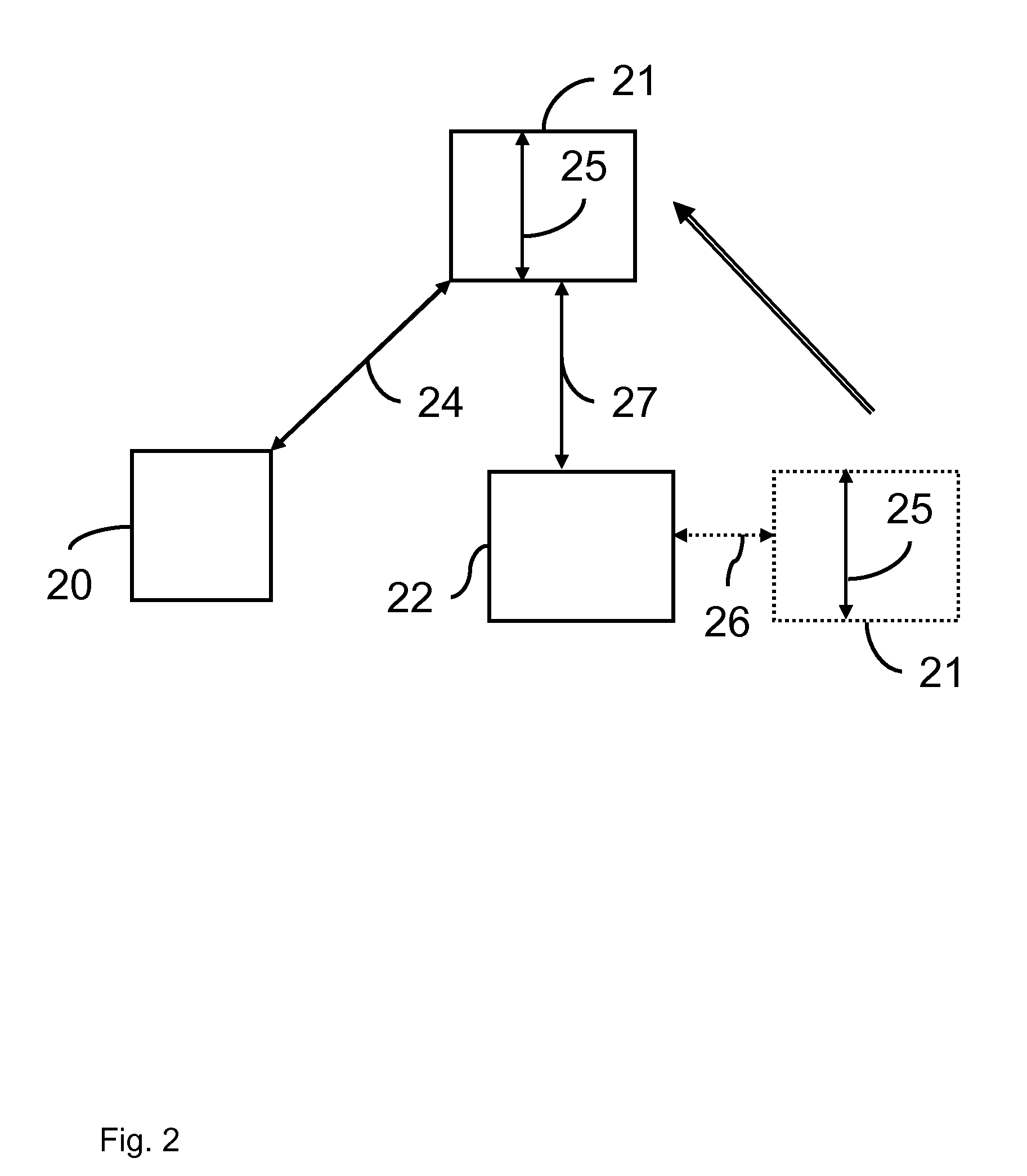
[0026]The method according to the invention takes advantage of the fact that interactions between direct neighbors are far more significant than interactions between other objects. When modifying a layout, especially the effects on the interactions between direct neighbors ar...
PUM
 Abstract
Description
Claims
Application Information