Communication device

a communication device and communication circuit technology, applied in the field of communication devices, can solve the problems of consuming a lot of power in the communication circuit, and achieve the effect of reducing the number of millimeter-wave band communication antennas and high degree of flexibility in layou

Active Publication Date: 2021-09-28
MURATA MFG CO LTD
View PDF9 Cites 0 Cited by
  • Summary
  • Abstract
  • Description
  • Claims
  • Application Information

AI Technical Summary

Benefits of technology

[0008]This configuration offers a high degree of flexibility in the layout of the one or more millimeter-wave band communication antennas and eases the constraints on the number of millimeter-wave band communication antennas to be provided. In the communication device having this configuration, the performance of the communication circuit for millimeter-wave band communication may be fully exploited.

Problems solved by technology

Communication circuits consume a lot of power particularly when carrying out communication in the submillimeter-wave and millimeter-wave bands, which may be used under limited conditions accordingly.

Method used


Image

  • Communication device
  • Communication device
  • Communication device

Examples


embodiment 1

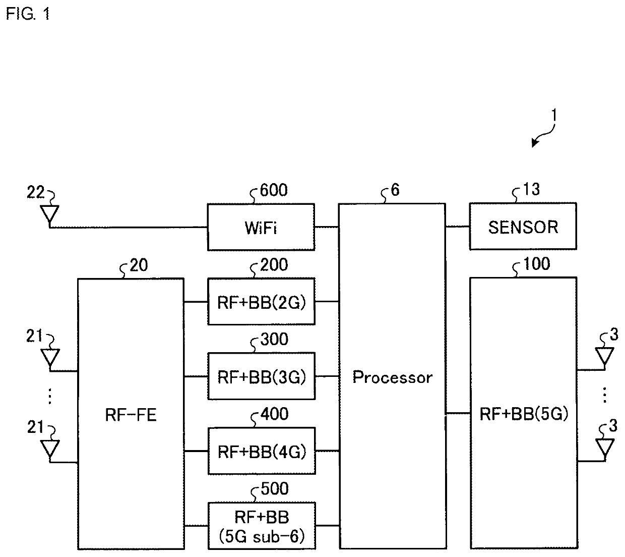
[0045]FIG. 1 is a block diagram illustrating the schematic configuration of a communication device according to Embodiment 1. As illustrated in FIG. 1, a communication device 1 according to the present embodiment includes a communication circuit (RF+BB (2G)) 200 for 2G, a communication circuit (RF+BB (3G)) 300 for 3G, a communication circuit (RF+BB (4G)) 400 for 4G, a communication circuit (RF+BB (5G sub-6)) 500 for 5G sub-6, a radio-frequency (RF) front-end circuit 20, radio-frequency (RF) antennas 21, a communication circuit 600 for WiFi communication, a WiFi antenna 22, a communication circuit 100 for 5G millimeter-wave band communication, millimeter-wave band communication antennas 3, a sensor 13, and a processor 6. According to the present disclosure, frequency bands for use in millimeter-wave band communication include, in addition to semimillimeter-wave and millimeter-wave bands such as 28 GHz band, 39 GHz band, and 60 GHz band, the following bands defined by IEEE: X-band (8 ...

embodiment 2

[0080]The first body 1A or the second body 1B of the communication device 1 includes a battery. In the body including the battery, the limited space is available for the millimeter-wave band communication antennas 3. When the millimeter-wave band communication antennas 3 are provided in the body that does not include a battery, the space in the smartphone may be well-utilized with no space wasted.

embodiment 3

[0081]FIG. 22A is a view of an exemplary RF module in the communication device according to Embodiment 3. FIG. 22B is a view of the RF module illustrated in FIG. 22A and seen in the direction of the arrow F.

[0082]As illustrated in FIG. 22A, the millimeter-wave band communication antenna 3c in the present embodiment is an array antenna including the patch antennas 3a arranged on the surface of a flexible substrate 3d. Each patch antenna 3a is a radiation conductor disposed on the surface of the flexible substrate 3d, which is so flexible that it can be bent as desired.

[0083]As illustrated in FIG. 22B, an RF module 7a is constructed in such a manner that the RFIC 4 is disposed on a back surface of the flexible substrate 3d, that is, the RFIC 4 is disposed on the surface opposite to the surface on which the patch antennas 3a are disposed.

[0084]Although FIGS. 22A and 22B illustrate an example in which the millimeter-wave band communication antenna 3c and the RFIC 4 are combined into the...


PUM


Abstract

A communication device includes: a first body including a first display portion; a second body including a second display portion; a communication circuit that carries out millimeter-wave band communication; and one or more millimeter-wave band communication antennas provided in at least one of the first body and the second body.

Description

[0001]This application claims priority from Japanese Patent Application No. JP2018-195347 filed on Oct. 16, 2018, and claims priority from Japanese Patent Application No. 2019-139090 filed on Jul. 29, 2019. The content of these applications are incorporated herein by reference in their entireties.BACKGROUND OF THE DISCLOSURE1. Field of the Disclosure[0002]The present disclosure relates to a communication device.2. Description of the Related Art[0003]Mobile communication terminals, such as mobile phones and mobile information terminals, wireless LAN terminals, and other communication devices that accommodate multi-standard (multi-mode) communications are available. These communication devices are provided with multiple communication systems supporting the second-generation mobile communication system (hereinafter also simply referred to as “2G”), the third-generation mobile communication system (hereinafter also simply referred to as “3G”), and the fourth-generation mobile communicat...

Claims


Application Information

Patent Timeline
Patent Type & Authority Patents(United States)
IPC IPC(8): H01Q1/24H04B7/0413H01Q1/22G06F1/16
CPCH01Q1/243G06F1/1616G06F1/1641G06F1/1647H01Q1/2266H04B7/0413G06F1/1698H01Q1/38H01Q21/065H01Q25/00
Inventor MIZUNUMA, RYUKENTANAKA, SATOSHIYAMAMOTO, YASUHISAITABASHI, AKIKO
Owner MURATA MFG CO LTD
Why Eureka
Try Eureka