Display device and method of controlling the same

a display device and control method technology, applied in the field of display devices, can solve the problems of reducing increasing the size and affecting the quality of the display device, so as to reduce the output load and mounting cost of the driving circuit, improve the image display quality, and reduce the number of output lines of the signal line driving circuit.

Active Publication Date: 2012-11-06
JOLED INC
View PDF41 Cites 6 Cited by
  • Summary
  • Abstract
  • Description
  • Claims
  • Application Information

AI Technical Summary

Benefits of technology

[0023]According to the display device and the method of controlling the same according to the present invention, the driving transistor initialization periods and the threshold voltage correction periods can be made uniform within a driving block, and thus the initialization period and the correction period can take a large part of a 1-frame period. With this, a precisely corrected drive current flows to the luminescence elements, and thus image display quality improves. In addition, the forming of driving blocks makes it possible to reduce the number of times that the signal level outputted by the driving circuit is switched in the aforementioned periods, and furthermore, with the selector provided between the signal line driving circuit and the signal lines, the number of output lines from the signal line driving circuit can be reduced. This allows for a reduction in driving circuit output load and mounting costs as well as improved manufacturing yield.

Problems solved by technology

Furthermore, the increase in the signal lines for each pixel row causes the number of outputs of the signal line driving circuit to increase, thereby causing an increase in the size and cost of the driving circuit and deterioration of manufacturing yield.
Furthermore, in the conventional display device disclosed in Patent Reference 1, the initialization period of the driving transistor and the correction period for the threshold voltage Vth is under 2 H, and thus there is a limitation for a display device in which high-precision correction is required.

Method used


Image

  • Display device and method of controlling the same
  • Display device and method of controlling the same
  • Display device and method of controlling the same

Examples


first embodiment

[0083]A first embodiment of the present invention will be described below with reference to drawings.

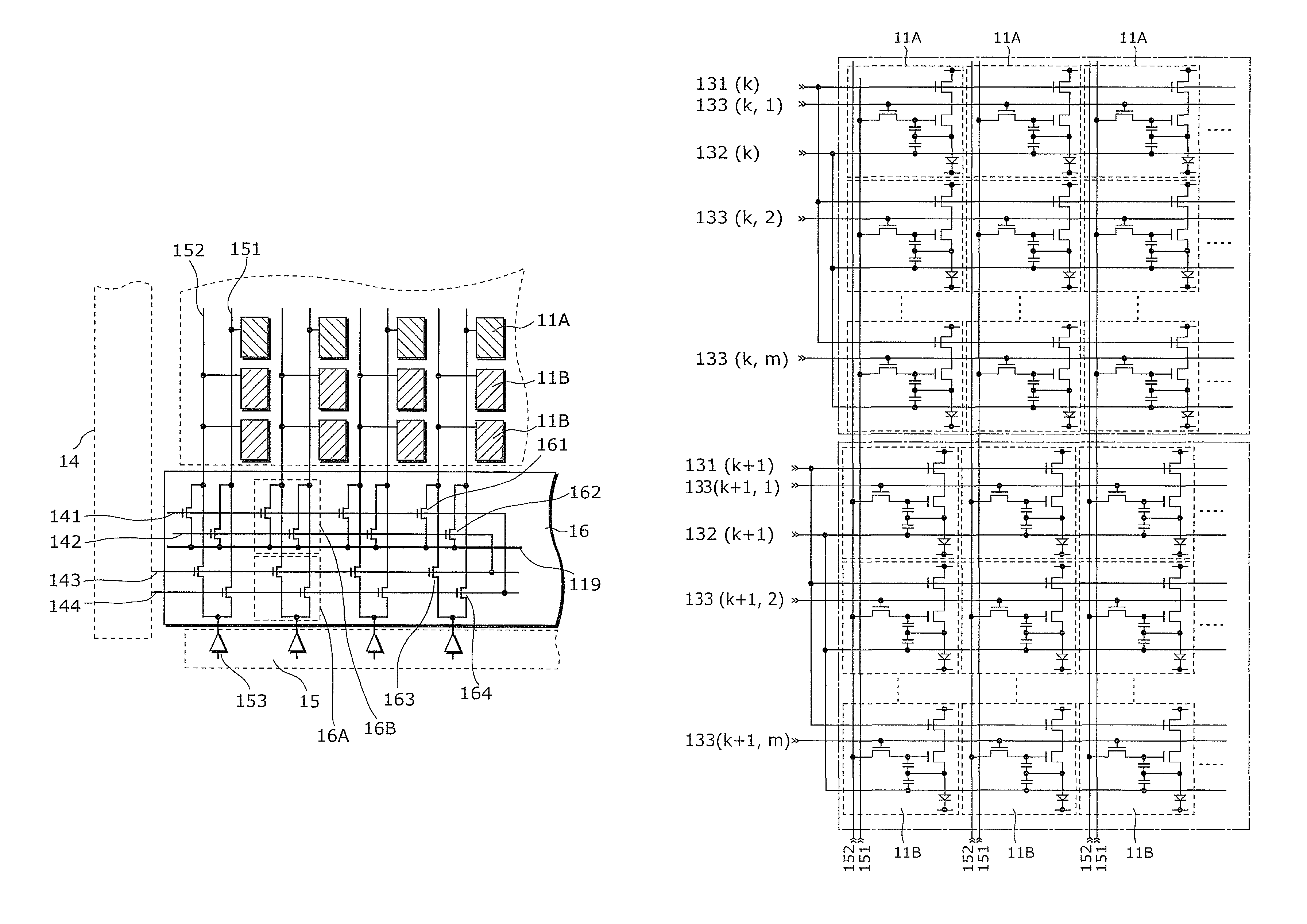
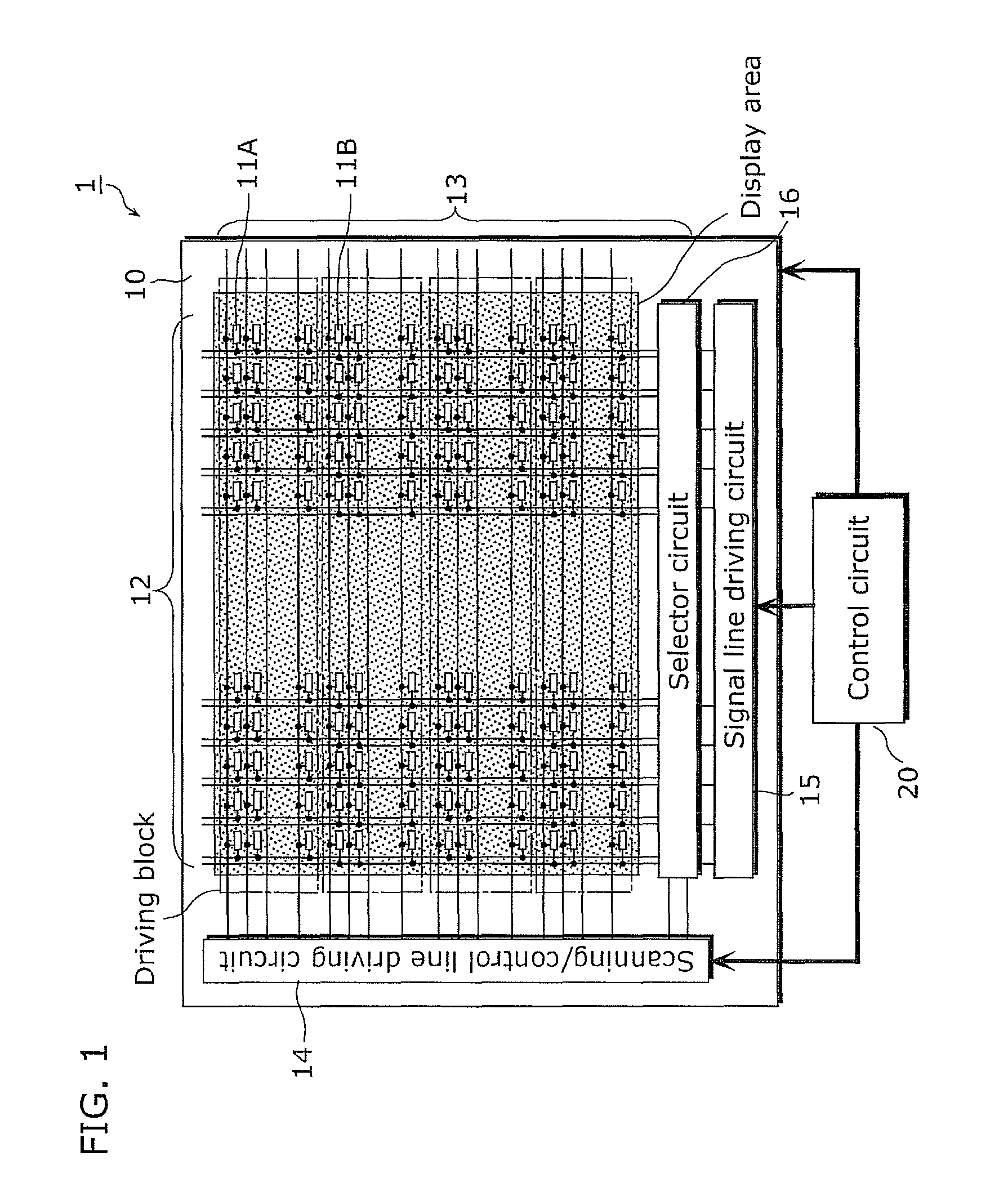
[0084]FIG. 1 is a block diagram illustrating an electrical configuration of a display device according to the first embodiment of the present invention. The display device 1 in FIG. 1 is a display device that has a plurality of pixels arranged in a matrix and includes a display panel 10 and a control circuit 20. The display panel 10 includes a plurality of pixels 11A and 11B, a signal line group 12, a set of control lines 13, a scanning / control line driving circuit 14, a signal line driving circuit 15, and a selector circuit 16.

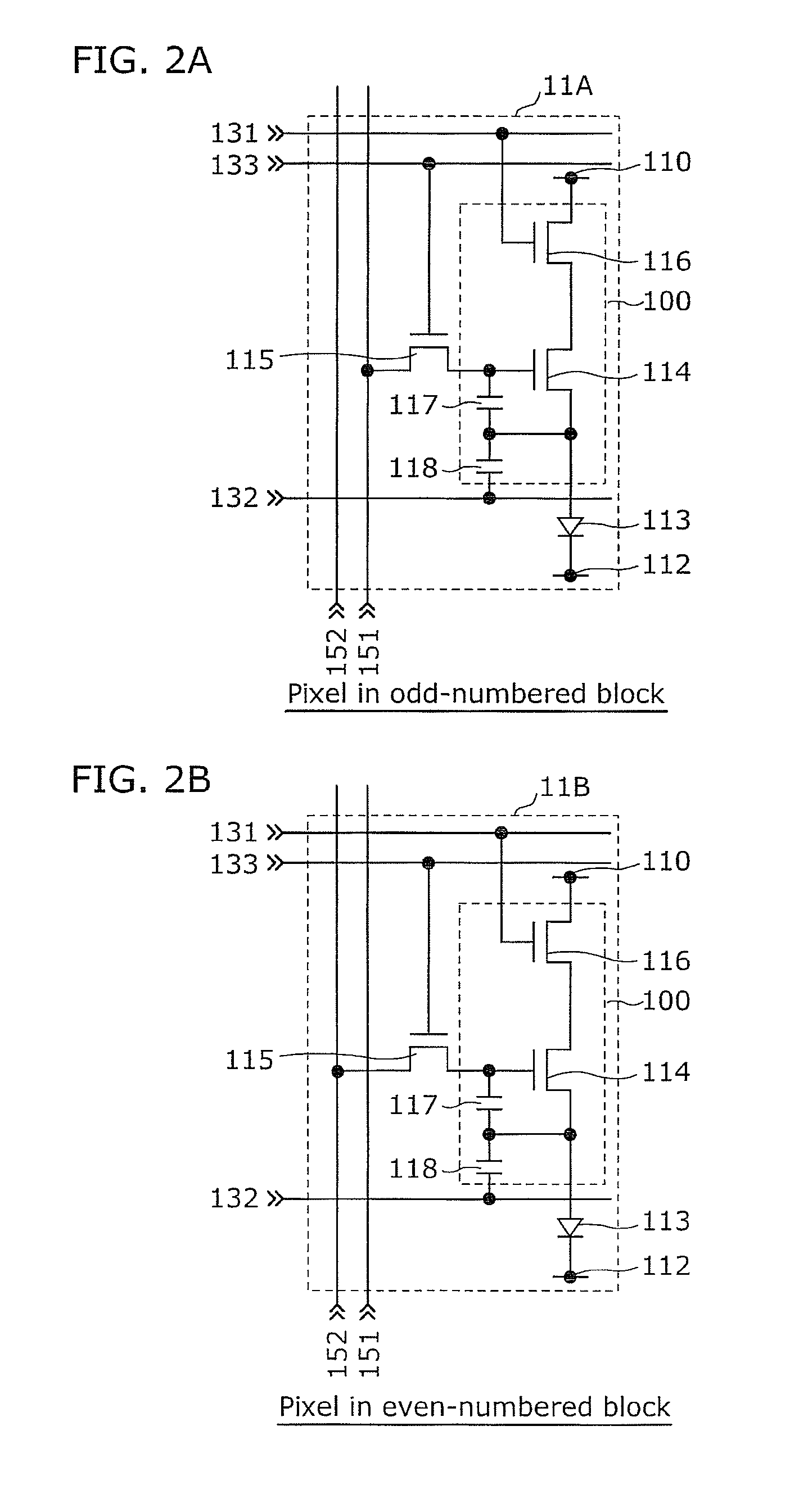
[0085]The pixels 11A and 11B are arranged in a matrix on the display panel 10. Here, the pixels 11A and 11B make up two or more driving blocks each including a plurality of pixel rows. Specifically, the pixels 11A make up a k-th driving block (where k is a natural number) and the pixels 11B make up a (k+1)-th driving block. This means that the pixels 11A make ...

second embodiment

[0199]A second embodiment of the present invention will be described with reference to drawings.

[0200]FIG. 12 is a circuit diagram illustrating a portion of a display panel of a display device according to the second embodiment of the present invention. FIG. 12 illustrates two adjacent driving blocks, control lines, scanning lines, and signal lines. The control lines, the scanning lines, and the signal lines are denoted by a reference numeral followed by (block number, row number in the block) or a reference numeral followed by (block number) in the figure and the following description.

[0201]Each pixel of the display device illustrated in FIG. 12 has the same circuit configuration that of the display device 1 according to the first embodiment. The only difference from the display device 1 of the first embodiment is that a second control line 131 in the display device of the second embodiment is not communized in each driving block but a second control line 131 in each pixel row is c...

third embodiment

[0239]Another embodiment of the present invention will be described below with reference to drawings.

[0240]An electrical configuration of a display device according to this embodiment is similar to the configuration illustrated in FIG. 1 with the only difference being the circuit configuration of each pixel.

[0241]Specifically, the display device according to this embodiment includes a display panel 10 and a control circuit 20. The display panel 10 includes a plurality of pixels 21A and 21B, which will be described later, a signal line group 12, a set of control lines 13, a scanning / control line driving circuit 14, a signal line driving circuit 15, and a selector circuit 16.

[0242]In the following, description of the same components as those of the first and second embodiments will be omitted and only components relating to the pixels 21A and 21B will be described.

[0243]The pixels 21A and 21B are arranged in a matrix on the display panel 10. Here, the pixels 21A and 21B make up two or...


PUM


Abstract

A display device including pixels has formed therein at least two driving blocks each made up of pixel rows, and includes: a signal line driving circuit that outputs a signal voltage to an output line disposed in each of pixel columns; and a selector circuit that provides a signal voltage outputted from the output line to one of a first signal line and a second signal line which are provided in each of the columns, provides a standard voltage from a standard voltage source to one of the two signal lines, and provides the signal voltage and the standard voltage mutually exclusively to the two signal lines. Each of the pixels includes a current control unit and an organic EL element. Pixels in the k-th driving block are connected to the first signal line and pixels in the (k+1)-th driving block are connected to the second signal line.

Description

CROSS REFERENCE TO RELATED APPLICATION[0001]This is a continuation application of PCT Patent Application No. PCT / JP2010 / 005466 filed on Sep. 6, 2010, designating the United States of America. The entire disclosure of the above-identified application, including specification, drawings and claims is incorporated herein by reference in its entirety.BACKGROUND OF THE INVENTION[0002](1) Field of the Invention[0003]The present invention relates to display devices and to methods of controlling the same, and particularly relates to a display device using a current-driven luminescence element and to a method of controlling the same.[0004](2) Description of the Related Art[0005]Display devices using organic electroluminescence (EL) elements are well-known as display devices using current-driven luminescence elements. An organic EL display device using such self-luminous organic EL elements does not require backlights needed in a liquid crystal display device and is best suited for increasing ...

Claims


Application Information

Patent Timeline
Patent Type & Authority Patents(United States)
IPC IPC(8): G09G3/30
CPCG09G3/3258H01L27/3276G09G2300/0819G09G2310/0218G09G2300/0852H10K59/131G09G3/30
Inventor MATSUI, MASAFUMIONO, SHINYA
Owner JOLED INC
Why Eureka
Try Eureka