Image display device and driving method thereof

a technology of image display device and driving method, which is applied in the direction of static indicating device, tubes with electrostatic control, instruments, etc., can solve the problem of high-precision correction limitation of image display device, and achieve the effect of reducing load, improving image display quality, and highly precise driving current flow

Active Publication Date: 2011-07-28
JOLED INC
View PDF16 Cites 30 Cited by
  • Summary
  • Abstract
  • Description
  • Claims
  • Application Information

AI Technical Summary

Benefits of technology

[0023]According to the image display device and the driving method thereof according to the present invention, the drive transistor threshold voltage correction periods as well as the timings thereof can be made uniform within a drive block, and thus the number of times that the signal level is switched from ON to OFF and from OFF to ON can be reduced and thus reducing the load on the driver which drives the respective circuits of the luminescence pixels. In addition, through the above-described forming of drive blocks and the two signal lines provided for each luminescence pixel column, the drive transistor threshold voltage correction period can take a large part of a 1-frame period, and thus a highly precise drive current flows to the luminescence elements and image display quality improves.

Problems solved by technology

Furthermore, in the conventional image display device disclosed in Patent Reference 1, the correction period for the threshold voltage Vth of the drive transistor is under 2 H, and thus there is a limitation for an image display device in which high-precision correction is required.

Method used


Image

  • Image display device and driving method thereof
  • Image display device and driving method thereof
  • Image display device and driving method thereof

Examples


first embodiment

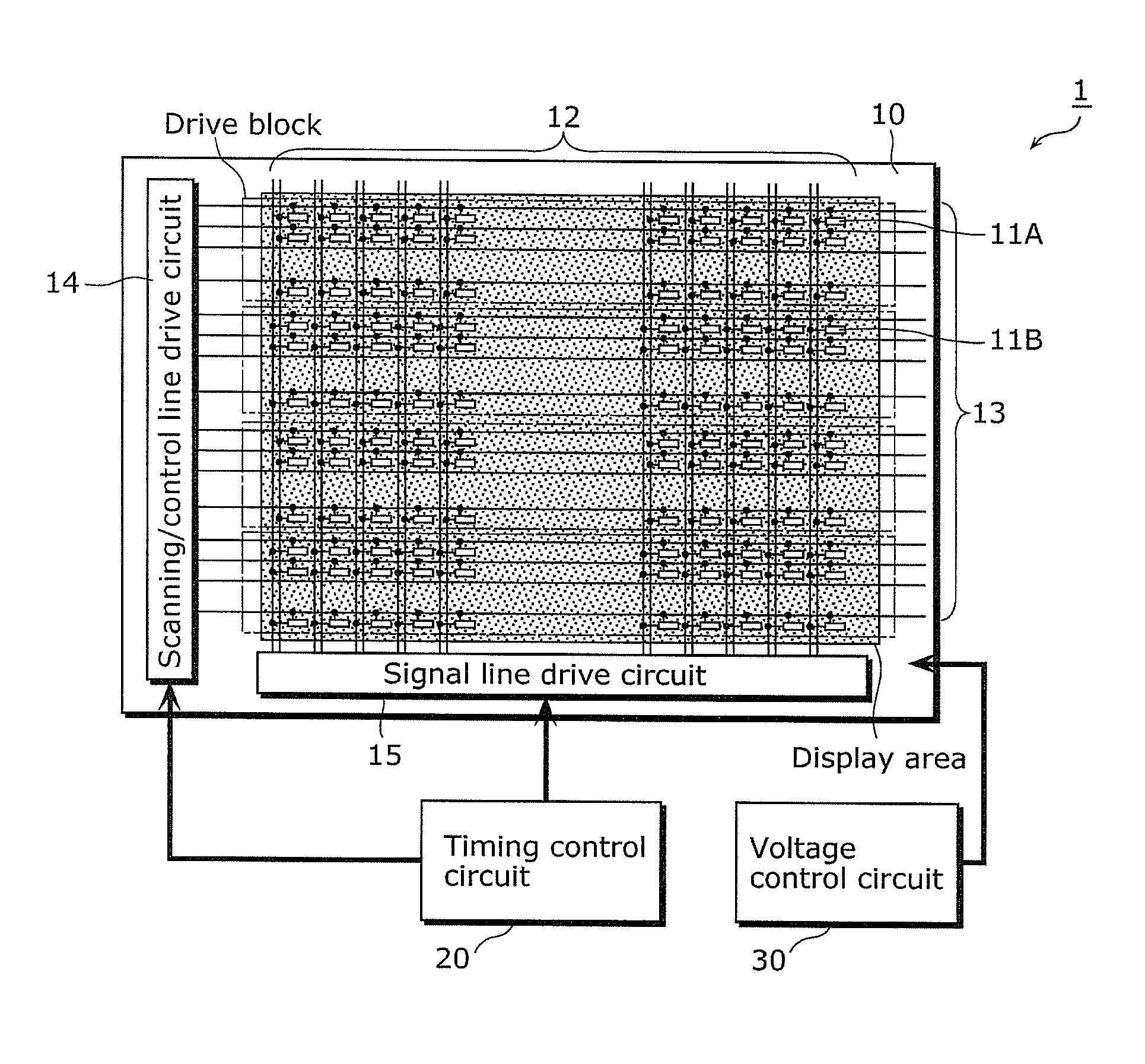
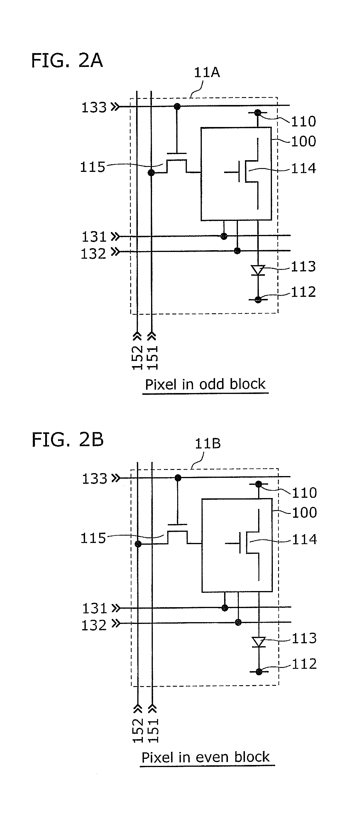
[0072]The image display device in the present embodiment is an image display device including luminescence pixels arranged in rows and columns, the image display device including: a first signal line and a second signal line each provided on a per luminescence pixel column basis; and a first control line provided on a per luminescence pixel column basis, wherein the luminescence pixels compose two or more drive blocks each including rows of the luminescence pixels, each of the luminescence pixels includes: a drive transistor; a first capacitor having both terminals connected to a gate and a source of the drive transistor; a luminescence element connected to the source of the drive transistor; a fourth switch which switches a drain current of the drive transistor ON and OFF; and a second capacitor provided between the source of the drive transistor and the first control line, each of the luminescence pixels that belong to a kth drive block (k is a positive integer) further includes a...

second embodiment

[0160]Hereinafter, an embodiment of the present invention shall be described with reference to the Drawings.

[0161]FIG. 10 is a circuit configuration diagram showing part of a display panel included in an image display device according to a second embodiment of the present invention. The figure shows two adjacent drive blocks and respective control lines, respective scanning lines, and respective signal lines. In the figure and the subsequent description, the respective control lines, respective scanning lines, and respective signal lines shall be represented by “reference number (block number; row number of the block)” or “reference number (block number)”.

[0162]Compared to the image display device 1 shown in FIG. 5, the image display device shown in the figure has the same circuit configuration for the respective luminescence pixels but is different in that the second control line 131 is not shared on a drive block basis and is connected on a per luminescence pixel row basis to the ...

third embodiment

[0204]The image display device in the present embodiment is a an image display device including luminescence pixels arranged in rows and columns, the image display device including: a first signal line and a second signal line each provided on a per luminescence pixel column basis; and a first control line provided on a per luminescence pixel column basis, wherein the luminescence pixels compose two or more drive blocks each including rows of the luminescence pixels, each of the luminescence pixels includes: a drive transistor; a first capacitor having two terminals with one of the terminals being connected to a gate of the drive transistor; a luminescence element connected to a source of the drive transistor; a third switch having one of a source and a drain connected to the other of the terminals of the first capacitor and the other of the source and the drain connected to the source of the drive transistor; and a second capacitor having two terminals with one of the terminals bei...


PUM


Abstract

An image display device includes luminescence pixels arranged in rows and columns. The image display device includes a first signal line and a second signal line, first control lines, and at least two drive blocks. Each drive block is composed of luminescence pixels in at least two of the rows. Each luminescence pixel includes a luminescence element and a current controller. Each of the luminescence pixels that belong to a kth drive block further includes a first switch provided between the first signal line and the current controller. Each of the luminescence pixels that belong to a (k+1)th drive block further includes a second switch provided between the second signal line and the current controller. Each of the first control lines is connected to all of the luminescence pixels in one of the drive blocks and not connected to the luminescence pixels in a different drive block.

Description

CROSS REFERENCE TO RELATED APPLICATION(S)[0001]This is a continuation application of PCT application No. PCT / JP2010 / 001536 filed on Mar. 5, 2010, designating the United States of America, the disclosure of which, including the specification, drawings, and claims, is incorporated herein by reference in its entirety.[0002]The disclosure of Japanese Patent Application No. 2009-054206 filed on Mar. 6, 2009 including the specification, drawings, and claims is incorporated herein by reference in its entirety.BACKGROUND OF THE INVENTION[0003]1. Field of the Invention[0004]The present invention relates to image display devices and driving methods thereof, and particularly to an image display device using current-driven luminescence elements, and a driving method thereof.[0005]2. Description of the Related Art[0006]Image display devices using organic electroluminescence (EL) elements are well-known as image display devices using current-driven luminescence elements. An organic EL display dev...

Claims


Application Information

Patent Timeline
Patent Type & Authority Applications(United States)
IPC IPC(8): G09G3/12H01J1/46
CPCG09G3/3233G09G2300/0819G09G2300/0852G09G3/12G09G2300/0876G09G2310/0218G09G2310/0221G09G2300/0861
Inventor ONO, SHINYA
Owner JOLED INC
Why Eureka
Try Eureka